
Basic Connection circuit diagram INA326 327 signals and power
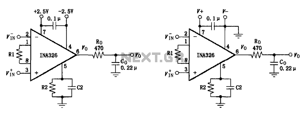
The INA326 and INA327 are precision instrumentation amplifiers designed for high accuracy and low noise applications. The circuit configuration emphasizes the importance of proper power supply decoupling to ensure optimal performance. The choice of a 0.1 µF capacitor for power supply filtering is critical, as it helps to minimize high-frequency noise and provides a stable voltage to the amplifier. The capacitor should be placed as close as possible to the power supply pins of the INA326/327 to reduce inductive effects from the circuit traces.
The output filter, consisting of Ro and Co, is designed to suppress any noise that may be present in the output signal. This filtering is essential when interfacing with sensitive components such as analog-to-digital converters, where noise can affect the accuracy of the digitized signal. The R2 // C2 network provides a ground-referenced output voltage, which is crucial for maintaining signal integrity in a mixed-signal environment.
The frequency response characteristics of the circuit are defined by the capacitors Co and C2, which create -3dB poles at 1 kHz, with each pole having a cutoff frequency of 1.5 kHz. This design ensures that the amplifier maintains a flat frequency response within the desired bandwidth, allowing for accurate signal processing.
The INA326/327 amplifiers are equipped with advanced technology that allows for exceptional common-mode rejection, which is particularly beneficial in environments where electrical noise and interference are prevalent. The ability to maintain a high CMR despite the presence of contact resistances, such as those found in socket connections, is a significant advantage. For applications requiring even better high-frequency common-mode rejection, the addition of a small capacitor between pins 1 and 8 can further enhance performance, allowing the amplifier to function effectively in high-frequency applications. This design consideration is vital for ensuring the integrity of the signal in high-speed data acquisition and processing systems. As shown for the basic connection circuit INA326/327 signals and power. Selection of the highest accuracy 0.1 F capacitor as power supply filtering, and should be as close to t he chip supply pin placement. Ro, Co is the output filter can filter out the noise output of the circuit; at the same time as the next stage input filter circuit, such as analog - digital converter input filter. R2 // C2 output voltage is ground referenced. Co and C2 joint formed at 1kHz frequency response of -3dB poles, each pole is 1.5kHz. And other instrumentation amplifiers, INA326/327 with a unique in-house technology to achieve excellent common-mode rejection ratio, and thus there is a connection during the contact resistance (such as socket contact resistance), does not make the common-mode rejection ratio is reduced.
In order to achieve better high-frequency CMR, you can add a small capacitor between 1,8 feet.
Related Circuits
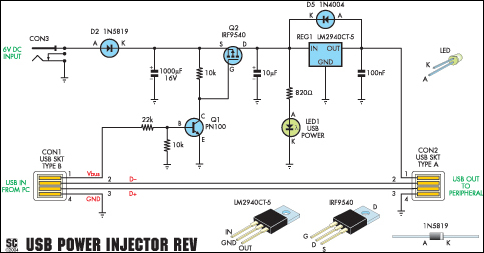
A portable USB hard drive is an effective means to back up data; however, issues may arise if the USB ports do not provide sufficient power to operate the drive. A modified version of the Silicon Chip USB Power...

This current-limiting circuit, illustrated as part of a small bench power supply, can be utilized with any dual-rail current source. The section of the circuit on the left limits the current entering the dual voltage regulator (IC4 to IC7)...
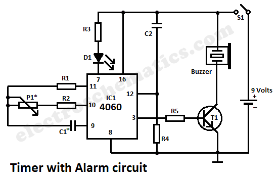
This simple alarm timer circuit is constructed using a 4060 integrated circuit, which features a stable oscillator with a relatively wide frequency range. The alarm timer circuit utilizes the CD4060 IC, which combines a low-frequency oscillator and a binary counter....
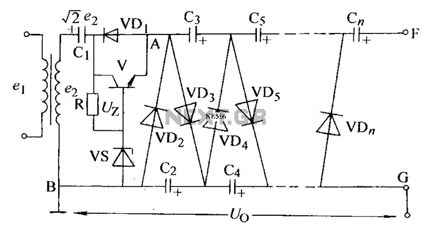
The circuit is an adjustable output voltage regulator type rectifier. It allows for obtaining peak voltage at odd multiples when the output voltage is taken from the circuit feedback (FB). Additionally, the lower point of the capacitor (CB) can...
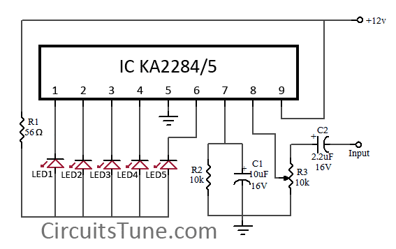
This is a simple circuit diagram of a 5-LED audio VU meter utilizing the ICs KA2284 or KA2285. The KA2284 and KA2285 are monolithic integrated circuits designed as logarithmic display driver ICs. They serve as bar-type display drivers for...
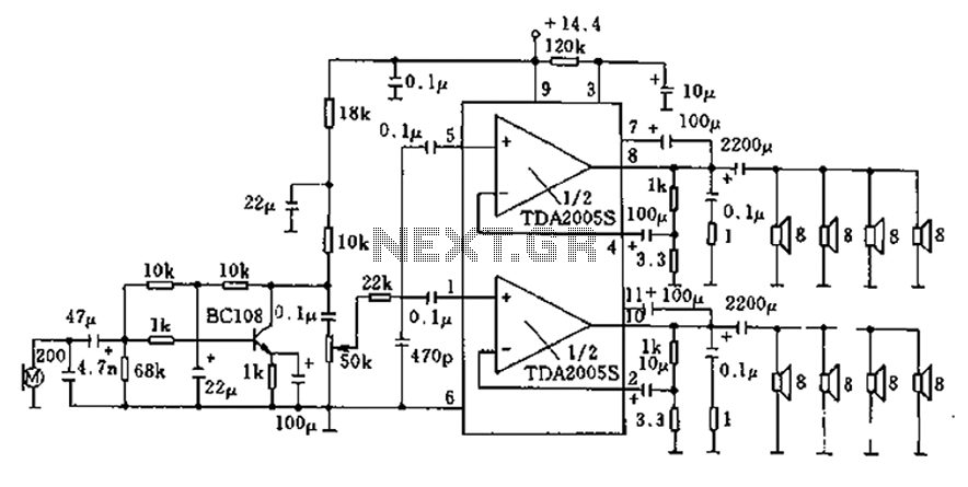
20W bus radio and megaphone circuit utilizing the TDA2005S double low-frequency power amplifier integrated circuit design. The front end can be connected to either a microphone input or a low-frequency radio output voltage amplification stage. Each TDA2005S provides 10W...