
0-50v 2a bench power supply
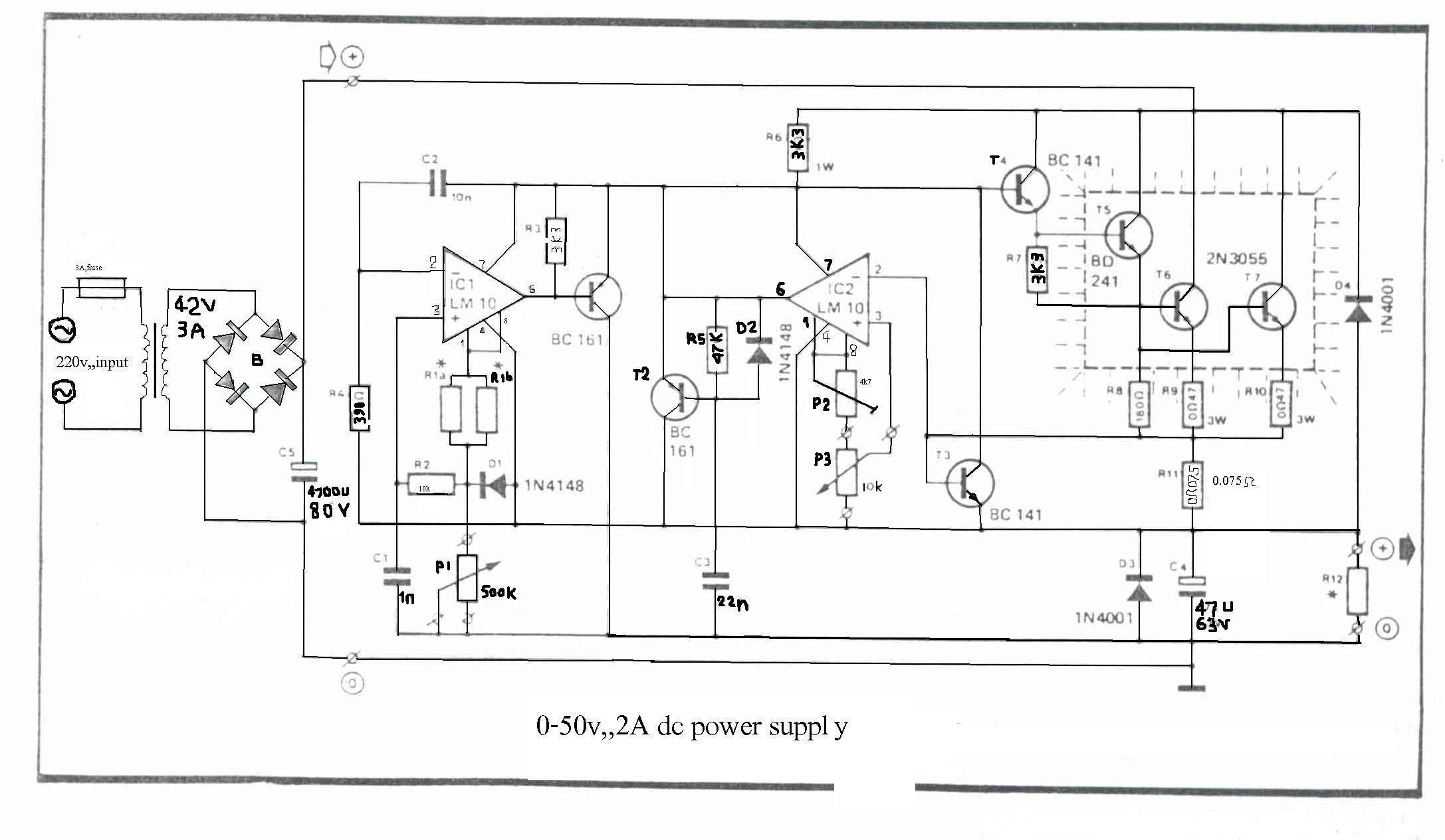
The circuit described utilizes the LM10 IC, which is designed to provide a stable reference voltage essential for regulating DC power supply applications. The configuration allows for flexibility in output voltage and current by integrating two LM10 ICs. The control of the output current, achieved through potentiometer P2, enables precise adjustments within the specified range of 0-2A, making the circuit adaptable for various load requirements.
The op-amp's negative and positive pins are critical for maintaining output voltage stability. Resistor R4, connected to the negative pin, works in conjunction with resistors R2 and P1 on the positive pin, ensuring that the op-amp operates effectively within its linear region. The control of voltage ripple is managed by transistor T1, which acts as a buffer and regulator, ensuring that the output remains stable despite variations in load conditions.
Transistor T1's role is pivotal, as it not only regulates the current through R6 but also influences the voltages at T5 and T4, which are essential for the overall performance of the circuit. The reference voltage established at pin 1 is critical for the operation of the entire system, as it serves as a benchmark against which the output is measured. The voltage drop across R1, which is set at a current of 100 µA, is essential for determining the effective output voltage.
The inclusion of transistor T3 for short circuit protection demonstrates a robust design approach, ensuring that the circuit can withstand fault conditions without sustaining damage. The design stipulates that a 470-ohm resistor be placed in parallel with the output to facilitate a reduction in output voltage to zero, thereby providing flexibility in operation.
The specifications for the transformer, which must deliver 36V at 3A, along with the use of a 4700 µF capacitor, indicate a well-thought-out power supply design capable of handling significant load variations. The requirement for heatsinks on transistors T6, T5, and T7 underscores the importance of thermal management in maintaining the reliability and longevity of the circuit components under varying operational conditions.I use the lm10 IC because it has a reference voltage and that`s useful for dc power supply. With two ICs can take different output voltage and amperage. This circuit is protected from short circuit. P2 is for controlling the current at the range of 0-2A. Stabilize the output voltage with R4 on negative pin on op-amp and with R2 & P1 on positive pin . Op-amp output controls T1 that not let ripple of voltage. T1 increase or decrease ampere of R6 and control the voltage of T5 & T4. Pin 1 is the reference voltage and reference voltage is losing some voltage on R1 that has 100uA. This current passes through P1 too. Vlose p1=100uA*Rp1 This lose voltage regulate output voltage rate of output current is compare between reference voltage of P3 and lose voltage on R11. T3 is protecting short circuit with R11. For reduce out put voltage to 0v should parallel one resistor 470 ohm in out put. Minimum voltage is 0. 4v. The maximum output voltage is fixed with R1b and should not become over of 50v. Therefore your transformer should give 36V, 3A with 4700uF capacitor. T6, T5, T7 need heatsilk. 🔗 External reference
Related Circuits
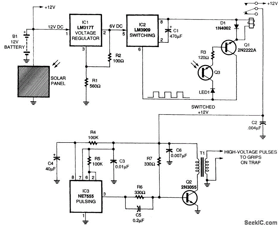
The circuit for the solar-powered controller includes a switching circuit, a pulsing circuit, and a high-voltage output circuit. The external power components consist of a 1- to 5-W solar panel and a 12-V motorcycle or camcorder battery. The output...
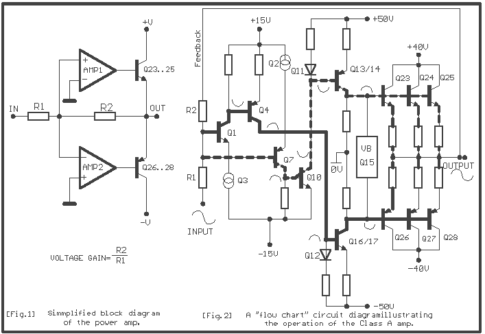
The simplified circuit [Fig.2] shows that each sub-amplifier consists of two voltage gain stages. The first stage consists of a complementary two stage common emitter [Q1-7] whose gain is about x2.3. The second stage is a current mirror stage [Q13-14]...
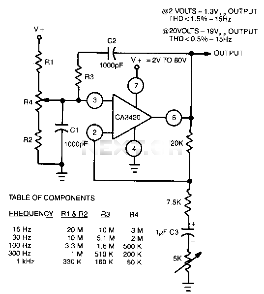
The adjustment of R4 contributes to the comparatively symmetrical output transfer characteristic of the CA3420 BiMOS operational amplifier. To extend the lower operating frequency, remove C3 and use a dual supply. The CA3420 is a high-performance BiMOS operational amplifier that...

The transformer has two primary windings and six secondary windings; the two 120-VAC primary windings and the 6.3-VAC secondary windings are connected in parallel. Modules A and B are identical; therefore, only the components of Module A are specified....
A simple Class B power amplifier can be constructed using the TDA8560 audio integrated circuit (IC). The TDA8560 amplifier features an internally fixed voltage gain, ensuring excellent channel balance. This audio amplifier project is capable of delivering dual 40-watt...
AN7112 power amplifier circuit diagram The AN7112 is a power amplifier designed for audio applications, capable of delivering high output power while maintaining high fidelity. The circuit diagram typically includes essential components such as transistors, resistors, capacitors, and a...