
0-50V 2A Bench power supply circuit and explanation
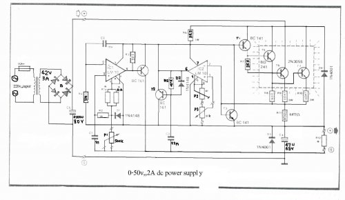
The circuit design primarily revolves around the LM10 IC, which serves as a voltage reference and an operational amplifier in this configuration. The dual usage of LM10 allows for flexibility in output specifications, enabling the user to achieve desired voltage and current levels tailored to specific applications. The inclusion of P2 for current control enhances the circuit's versatility, allowing for adjustments between 0 to 2A, which is crucial for various load requirements.
The stabilization of output voltage is a critical aspect of this design. The resistors R4, R2, and P1 work in unison to ensure that the output remains steady despite fluctuations in load. The op-amp output's influence on transistor T1 is vital as it acts as a regulator, preventing voltage ripples that could adversely affect downstream components. The ability of T1 to modulate the current through R6 plays a significant role in maintaining the desired operational parameters.
The reference voltage management is also noteworthy; the voltage drop across R1 creates a feedback mechanism that helps maintain the output voltage. The interaction between P3, which establishes a comparison point, and the voltage drop across R11 ensures that the circuit can react dynamically to changes in load conditions, providing robust performance.
In terms of safety, the inclusion of T3 and R11 for short-circuit protection is essential in preventing potential damage to the circuit. This feature enhances the reliability of the power supply, making it suitable for sensitive applications where overcurrent conditions may occur.
The output voltage range is well-defined, with a minimum of 0.4V and a maximum limit of 50V, dictated by R1b. This range allows for a wide variety of applications, from low-voltage devices to those requiring higher voltage levels. The specification of a transformer providing 36V at 3A, along with a significant capacitance of 4700 µF, indicates a design that can handle substantial load demands while maintaining stability.
Finally, the thermal management of the transistors T6, T5, and T7 is emphasized, as these components will dissipate heat during operation. Adequate heat sinking is necessary to ensure reliable operation and longevity of the circuit, particularly under high load conditions.I use the lm10 IC because it has a reference voltage and that`s useful for dc power supply. With two ICs can take different output voltage and amperage. This circuit is protected from short circuit. P2 is for controlling the current at the range of 0-2A. Stabilize the output voltage with R4 on negative pin on op-amp and with R2 & P1 on positive pin . Op-amp output controls T1 that not let ripple of voltage. T1 increase or decrease ampere of R6 and control the voltage of T5 & T4. Pin 1 is the reference voltage and reference voltage is losing some voltage on R1 that has 100uA. This current passes through P1 too. This lose voltage regulate output voltage rate of output current is compare between reference voltage of P3 and lose voltage on R11. T3 is protecting short circuit with R11. For reduce out put voltage to 0v should parallel one resistor 470 ohm in out put. Minimum voltage is 0. 4v. The maximum output voltage is fixed with R1b and should not become over of 50v. Therefore your transformer should give 36V, 3A with 4700uF capacitor. T6, T5, T7 need heatsilk. 🔗 External reference
Related Circuits
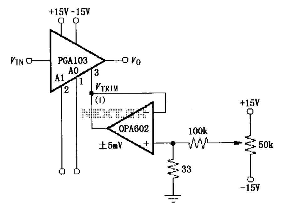
The PGA103 offset voltage correction circuit is designed to minimize the offset voltage for the PGA103 laser correction, ensuring that the gain for three typical offset voltage levels (relative to input) remains below 200 V. Each gain is associated...
This circuit is not visually appealing nor easy to implement, requiring considerable effort. The stepper motor consists of two coils, necessitating the use of two LMD18245 chips to manage the current flow through these coils. It is noteworthy that...
A simple motor control project for forward and backward drive can be implemented using the LB1948M motor driver IC, which features two channels for motor control. The LB1948M is an ideal choice for 12V motor drive systems and can...
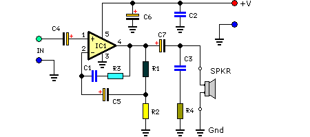
This compact amplifier is built around the TDA2003 integrated circuit, which can deliver 4W RMS at a 4-ohm load. The TDA2003 offers enhanced performance while maintaining the same pin configuration as the TDA2002. It retains the advantageous features of...
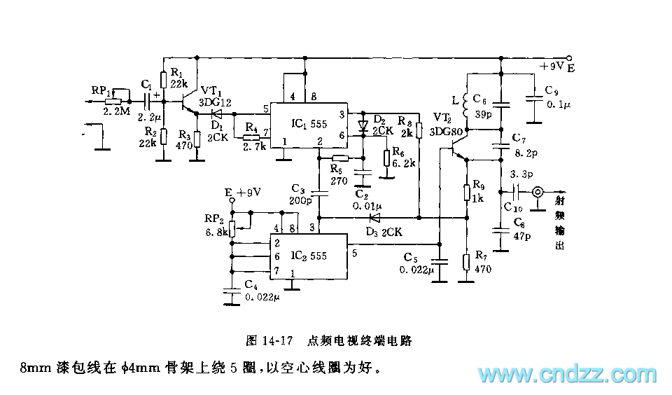
As shown in figure 14-17, this circuit consists of the input circuit, the line frequency synchronization generator, the sample-and-hold circuit, the voltage control delay generator, and the RF modulator. The input circuit includes the input attenuator RP1 and the...
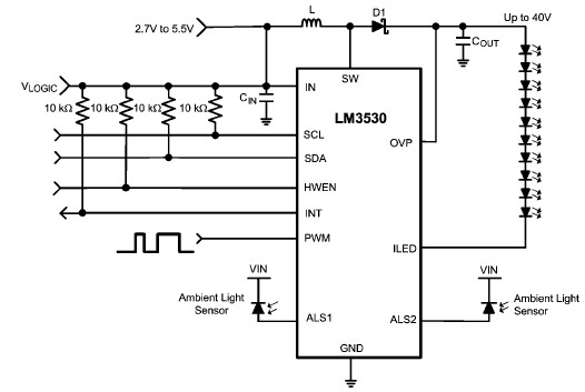
A simple white LED driver circuit can be designed using the LM3530 high-efficiency white LED driver IC, which features programmable ambient light sensing capability and an I2C compatible interface. The LM3530 LED driver can control up to 11 series...