
120W power amplifier circuit
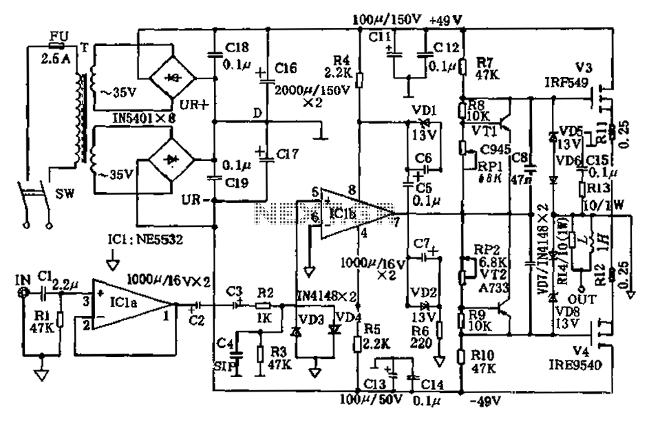
The described amplifier circuit utilizes a floating power supply to enhance output power capabilities, making it suitable for various applications where increased amplification is required. The use of an input voltage follower configuration (ICLA) ensures that the circuit maintains high input impedance, which is critical for interfacing with different signal sources without loading them down. The design's stability is further reinforced by the all-transistor closed-loop architecture, which minimizes the risk of self-oscillation and allows for high open-loop gain.
The inclusion of a capacitor (C4) at the non-inverting terminal of ICLB is particularly noteworthy, as it serves to extend the frequency response of the amplifier. This characteristic is essential for applications that demand fidelity across a broader frequency range, such as audio amplification or RF signal processing. The floating power loop established by components R6, C6, and C7 supports the operational amplifier's performance, ensuring that it can operate effectively within the desired frequency range.
The output stage bias circuit, composed of VT1, VT2, R7, R8, and R9, is designed to maintain optimal operating conditions for the output transistors. This biasing arrangement is crucial for preventing thermal runaway and ensuring consistent performance under varying load conditions. The gate protection circuit formed by F_T and F_KU provides an additional layer of safety for the output transistors, safeguarding them against voltage spikes that could lead to damage.
Overall, the amplifier circuit's design principles and component choices reflect a comprehensive approach to achieving high performance, stability, and versatility in amplification applications.Amplifier circuit of this paper is to introduce a floating power supply, the purpose is to increase the output power, the amplifier output power with only the final stage ampli fier supply voltage and casts about. Its principle is shown 2--116 shown. Iclt) as a pre-stage, ICla composition as the input voltage follower circuit, the purpose is to increase the input impedance, and to facilitate a variety of sources are connected. Its voltage gain of 1, is conducive to stable operation of the circuit o circuit input is suspended, the power stage, IClb inverting input voltage follower Icl group also be suspended.
This circuit is equivalent to the whole big closed loop of all-trans -fed, or that the whole closed loop of l, which makes the circuit very stable and, in any case does not appear self-excited. Closed loop feedback in turn means that the whole machine high open loop gain, the open loop gain of the unit up to lOOdB above.
Therefore, even if the final stage amplifier tube mismatch, it also minimal distortion oIClb noninverting terminal of the capacitor C4 is introduced to broaden the high frequency band, so that it reaches 60kHZo where ~ R6, C6, C7 op amp IClb floating power loop, vTl, VT2 and R7 ~ Rio and RPi, touch 2 group into the output stage bias circuit, f t ~ f Kui form the output pipe gate protection circuit.
Related Circuits
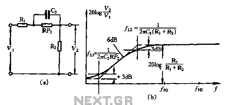
There are two corner frequencies present: the start frequency attenuation transition is defined by several parameters, including F1/27rC3 (Ri + R2). This is followed by a decay into a flat corner frequency, denoted as LI, which is represented by...

22W into 4 Ohm power amplifier, Variable Low Pass Frequency: 70-150Hz. This unit is intended to be connected to an existing car stereo amplifier, adding functionality. The described power amplifier is designed to deliver an output power of 22 watts...
A buzzer circuit utilizes a PIC microcontroller to drive a piezo buzzer. The microcontroller is a low-power processor that is ideal for portable and compact devices where battery conservation is essential. The buzzer circuit employs a PIC microcontroller, which serves...

This project involves a compact, portable DJ mixer that can be powered by a 9V DC external supply adapter or a 9V PP3 battery. The mixer includes two stereo phono inputs, two stereo line-level inputs, and a single stereo...
To achieve optimal performance as a low noise, high input impedance device, the preamplifier and tone control utilize JFET technology. The circuit is designed to minimize harmonic distortion levels. The use of Junction Field Effect Transistors (JFETs) in the preamplifier...
The TDC1808/TDC1809 is a pair of wireless remote control transmitter and receiver components. They utilize an internal antenna to transmit both digital and analog signals. These components are suitable for various wireless remote control devices. Key features include compact...