
12V Inverter Circuit Using 4013
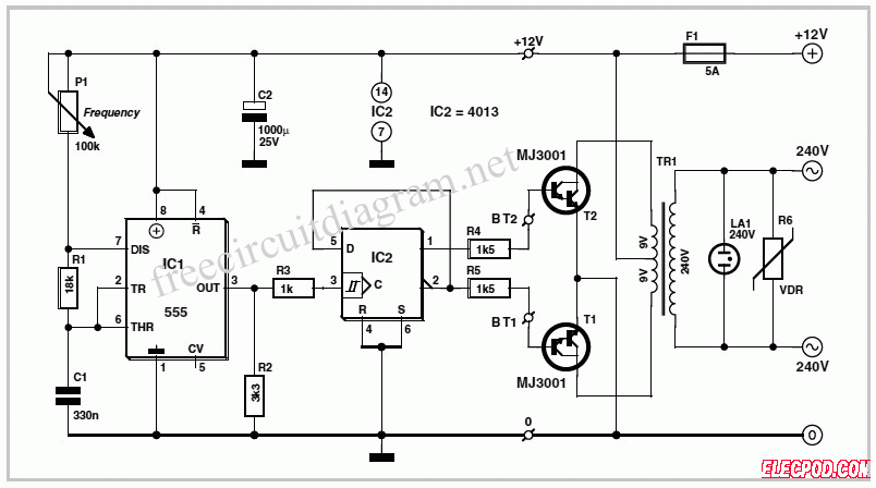
The 12V inverter circuit operates by converting a low voltage DC input into a high voltage AC output, which is essential for powering devices that require 230V AC. The astable multivibrator configuration of the 555 timer generates a continuous square wave signal, which is critical for the operation of the inverter. The frequency of this signal can be adjusted via the potentiometer, allowing for fine-tuning of the output waveform.
The CMOS 4013 flip-flop receives the square wave signal from the 555 timer and produces two complementary outputs. These outputs are essential for driving the Darlington transistors, which are configured in a push-pull arrangement to amplify the current. The MJ3001 transistors, known for their high gain and ability to handle significant current loads, are ideal for this purpose. They ensure that sufficient current is supplied to the transformer, allowing it to step up the voltage to the desired 230V AC level.
The transformer plays a crucial role in this circuit. By being used in reverse, it converts the low-voltage high-current output from the transistors into a high-voltage low-current output. The center-tapped design of the transformer provides two equal voltages, which are combined to produce the required AC output.
To ensure the safety and reliability of the circuit, a neon indicator light is included to signal the presence of the high voltage output. Additionally, the VDR acts as a protective element, absorbing transient voltage spikes that could otherwise damage the transistors or other components in the circuit.
Overall, this 12V inverter circuit is a practical and efficient solution for converting DC to AC power, making it a valuable project for electronics enthusiasts looking to explore inverter technology.This circuit is a circuit diagram 12V inverter is very easy to build, cheap components that many electronics hobbyists may even already have. Though it is possible to build a more powerful circuit, the complexity caused by the very heavy currents to be handled on the low-voltage side leads to circuits.
The circuit diagram of 12v inverter is easy t o follow. A classic 555 timer chip, identified as IC1, is configured as an astable multivibrator at a frequency close to 100 Hz, which can be adjusted accurately by means of potentiometer P1. It is used to drive a D type flip-flop produced using a CMOS type 4013 IC. This produces perfect complementary squarewave signals (in antiphase) on its Q and Q outputs suitable for driving the output power transistors.
The following is a schematic drawing: As the output current available from the CMOS 4013 is very small, Darlington power transistors are used to arrive at the necessary output current. We have chosen MJ3001s from the now defunct Motorola (only as a semi-conductor manufacturer, of course!) which are cheap and readily available, but any equivalent powerDarlington could be used.
These drive a 230 V to 2 G— 9 V centre tapped transformer used backwards` to produce the 230 V output. The presence of the 230 VAC voltage is indicated by a neon light, while a VDR (voltage dependent resistor) type S10K250 or S07K250 clips off the spikes and surges that may appear at the transistor switching points.
🔗 External reference
Related Circuits
Twang is a guitar sound that closely resembles that of a banjo or mandolin. The circuit generates distinctive sounds from a standard electric guitar by eliminating the bass frequencies, heavily distorting the midrange and treble frequencies, and subsequently amplifying...
The circuit operates using the MQK-2 gas sensor, which detects the presence of combustible gases or smoke through surface adsorption. When gas is detected, the inter-electrode resistance (BL) decreases significantly. This change in resistance affects the voltage at node...
Circuit for Grundig 5441 TV. If there are any issues related to this circuit, please provide additional information about the problem for further assistance. By accessing the Fixya site, users acknowledge that they have read and agreed to its...

A diode, such as the IN4148, has a typical temperature coefficient of -2 mV/°C at a 1 mA diode current. Transistors Q1 and Q2 form a constant current source. Diode D1 serves as the temperature sensor. Integrated circuits ICl-a...
A sine wave oscillator can be implemented using a Wien-Bridge oscillator, similar to the previous sine wave oscillator circuit; however, another method is now presented. The Wien-Bridge oscillator is a type of electronic oscillator that generates sine waves. It is...

The noise limiter circuit features a preamplifier clipper and a switchable audio bandpass filter. Audio levels ranging from 5 to 50 mV are amplified in a preamplifier to several volts peak-to-peak, which are then sent to a clipper and...
Warning: include(partials/cookie-banner.php): Failed to open stream: Permission denied in /var/www/html/nextgr/view-circuit.php on line 713
Warning: include(): Failed opening 'partials/cookie-banner.php' for inclusion (include_path='.:/usr/share/php') in /var/www/html/nextgr/view-circuit.php on line 713