
13.8V 20A power supply
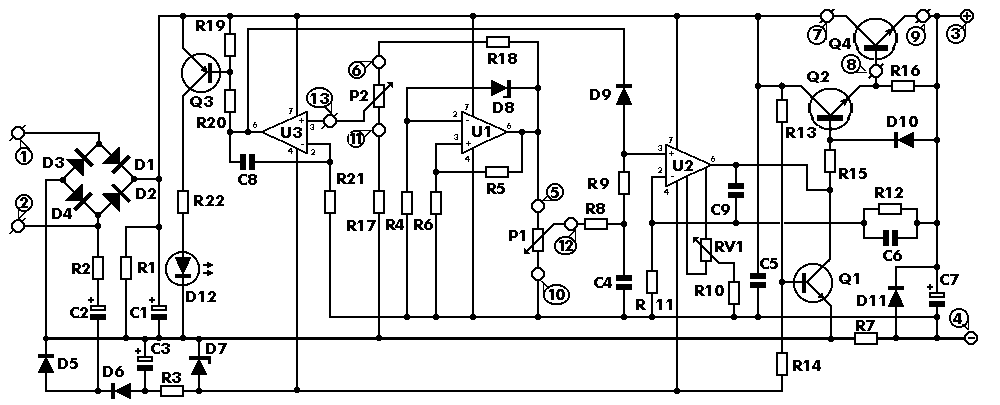
This is a PNP transistor (Ic>25) and current amplification factor of at least 20. The one that has been tested and proven here is the 2N5683. The current limiting resistance RL, for the maximum output of 20 Amps should be 0. 03 Ohms, rated at least 15W. You can use the resistance wire or switch several resistors in parallel, totaling the resistance/power values. Values for other currents can be calculated by the rule: The RL and Q2 (3A PNP such as BD330) form a short circuit automatic fuse .
As soon as the maximum current reaches 20Amps, the voltage drop over the resistor RL will open Q2, and thus limit the B-E Current of Q3. Parallel to Q2 is Q1, which lights the LED 1 whenever the current limiting circuit is active. When the fuse is active, the Q2 bridges the R3, so the full current would flow through the IC1, and damage it.
Therefore the R4 is inserted, as to limit the IC1 current to 15mA. This makes it possible to run the IC1 without any cooling aid. The LED 2 will light up every time the PSU is switched on. This circuit is very simple too. You will notice that there is no current sensing resistor. But it is really there, in a form of the Rds-on resistance of the N-channel FET, which actually handles the load cutoff from the source. The function of the FET is shown in the diagram 2. When the current Id is rising, the tension Uds over the resistance Rds rises very slowly in the beginning, but very fast after the knick.
This means, that before the knick the FET behaves as a resistor but after it, works as constant current source. The D2, R3 and B-E connection of the Q4 will sense the Uds voltage of the FET1. When the voltage rises enough, the Q4 will shortcut the FET1 gate to mass, and cut the current flow through the FET 1 off.
However, to enable the FET1 to open, there is certain gate voltage necessary, which in this case is brought up by the voltage divider consisting of R8, Z1, P1 and R9. So the maximum Gate voltage will be the one of the Z1, and the minimal will be around 3V6. The Z1 voltage (Uz1) will thus determine the max current flowing through the FET 1. The diagram 2 will show that for 5 Amps the Uz1 should be 5V6, and for 20Amps around 9V6. The Capacitor C4 will determine the velocity or the reaction time of the limiter. 100 uF will make the reaction time to be around 100ms, and 1n will make it 1us. Within the designed limits, the P1 will limit the current output in the range of 15mA to 20A. You can use both output simultaneously, but the total output current will be limited by the value of the RL.
This PSU can be built also for higher outputs, as long as the transformer will handle the current requirements, and you provide sufficient cooling for the Q3. 🔗 External reference
Related Circuits
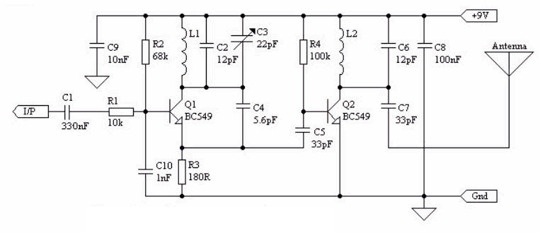
This low power FM transmitter is designed to utilize an input from another sound source and transmits on the commercial FM band. The transmitter is relatively powerful for its category. The first stage consists of an oscillator, which is...
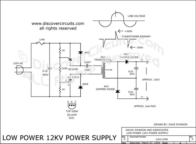
For generating approximately 12,000 volts DC for an ion generator, this circuit design may be suitable. It draws power from a 120 VAC power line and utilizes a small 6 kV camera flash trigger coil. The output signal is...
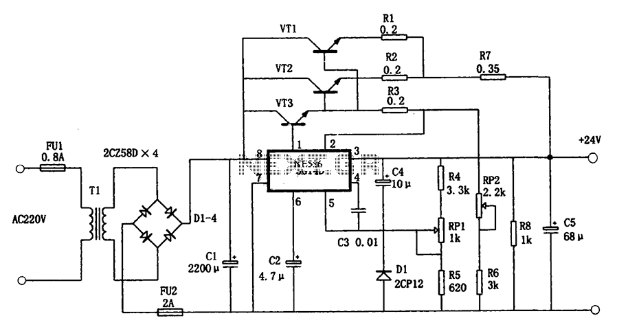
The circuit illustrated in the figure is a +24V, 1.9A power supply design. It employs the 5G14D domestic integrated voltage regulator as the core component, supported by three external power transistors. While the 5G14D voltage regulator has a rated...
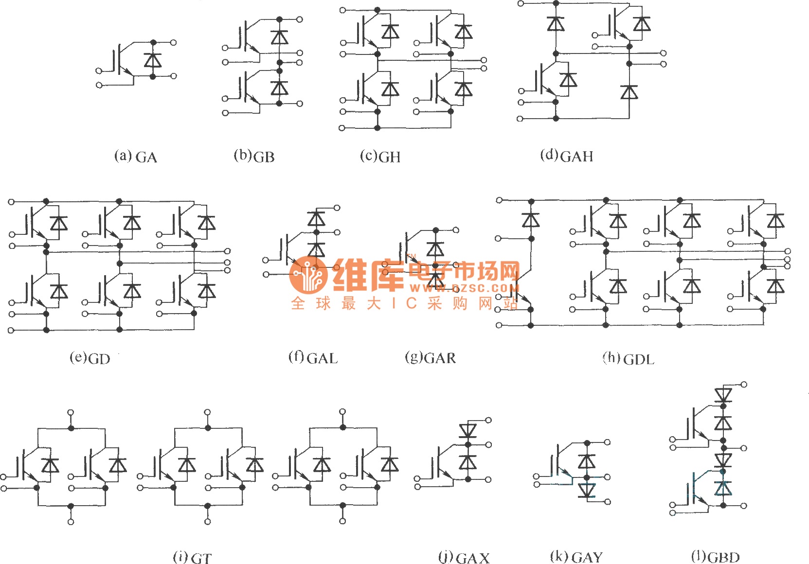
This document describes various electronic modules, including: (a) a single switch module; (b) a two-unit half bridge module; (c) an H bridge (single-phase bridge) module; (d) an asymmetrical H bridge module; (e) a three-phase bridge (six-unit or inverter bridge)...
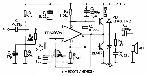
The rDA2030A TDA2030 is an enhanced version of the original product, with a maximum working voltage increased to 18V and a maximum output power of 18W. Additionally, harmonic distortion has been significantly reduced. The application circuit is illustrated. The rDA2030A...
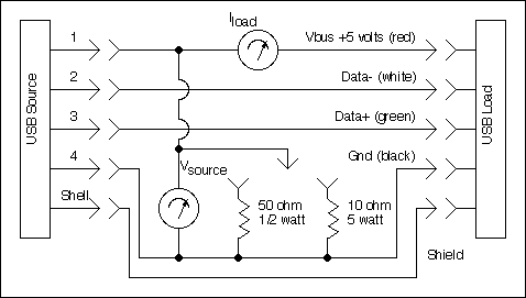
The Universal Serial Bus (USB) has become a popular method for connecting computer peripherals. The original USB 1.1 specification limited data rates to approximately 12 Mbits/sec, while the updated USB 2.0 specification increases these rates to up to 480...