
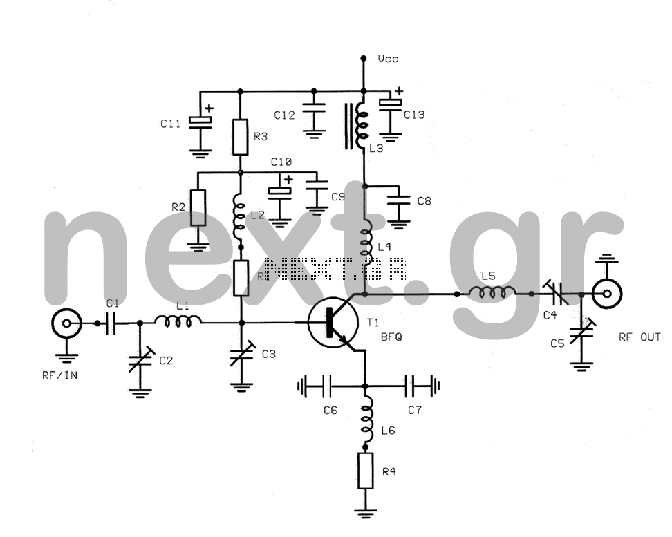
200Mhz cascode amplifier
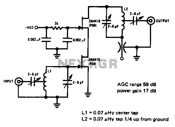
The 200 MHz JFET cascode circuit is designed to enhance performance in high-frequency applications while minimizing unwanted interactions between signals. The cascode configuration, which consists of two JFETs arranged in series, effectively increases the overall gain and bandwidth of the circuit. The lower JFET operates as the input stage, while the upper JFET serves as a cascode stage that isolates the lower device from the output load, thereby reducing the Miller effect and enhancing stability.
Low cross-modulation is a critical feature of this circuit, as it ensures that the presence of one signal does not adversely affect the amplification of another signal. This characteristic is particularly valuable in communication systems where multiple signals may be present simultaneously. The ability to handle large signals without distortion is achieved through careful biasing and selection of JFETs, ensuring that the devices operate within their optimal range.
The absence of neutralization simplifies the circuit design and reduces the potential for instability that can arise from feedback loops. Instead, the circuit relies on AGC to maintain consistent output levels despite variations in input signal strength. The biasing of the upper cascode JFET is crucial for controlling the gain and ensuring that the circuit responds appropriately to changes in signal amplitude.
The requirement that the Idss of the upper JFET be greater than that of the lower JFET is essential for maintaining the desired operating conditions. Idss, or the drain-source saturation current, influences the transconductance and overall gain of the JFET. By ensuring that the upper JFET has a higher Idss, the circuit can achieve better performance and stability, particularly in high-frequency applications where signal integrity is paramount.
Overall, this JFET cascode circuit is an effective solution for applications requiring high-frequency amplification with minimal distortion and robust performance under varying signal conditions.This 200 MHz JFET cascode circuit features low cross-modulation, large signal handling ability, no neutralization, and AGC controlled by biasing the upper cascode JFET The only special requirement of this circuit is that Idss of the upper unit must be greater than that of the lower unit. 🔗 External reference
Related Circuits
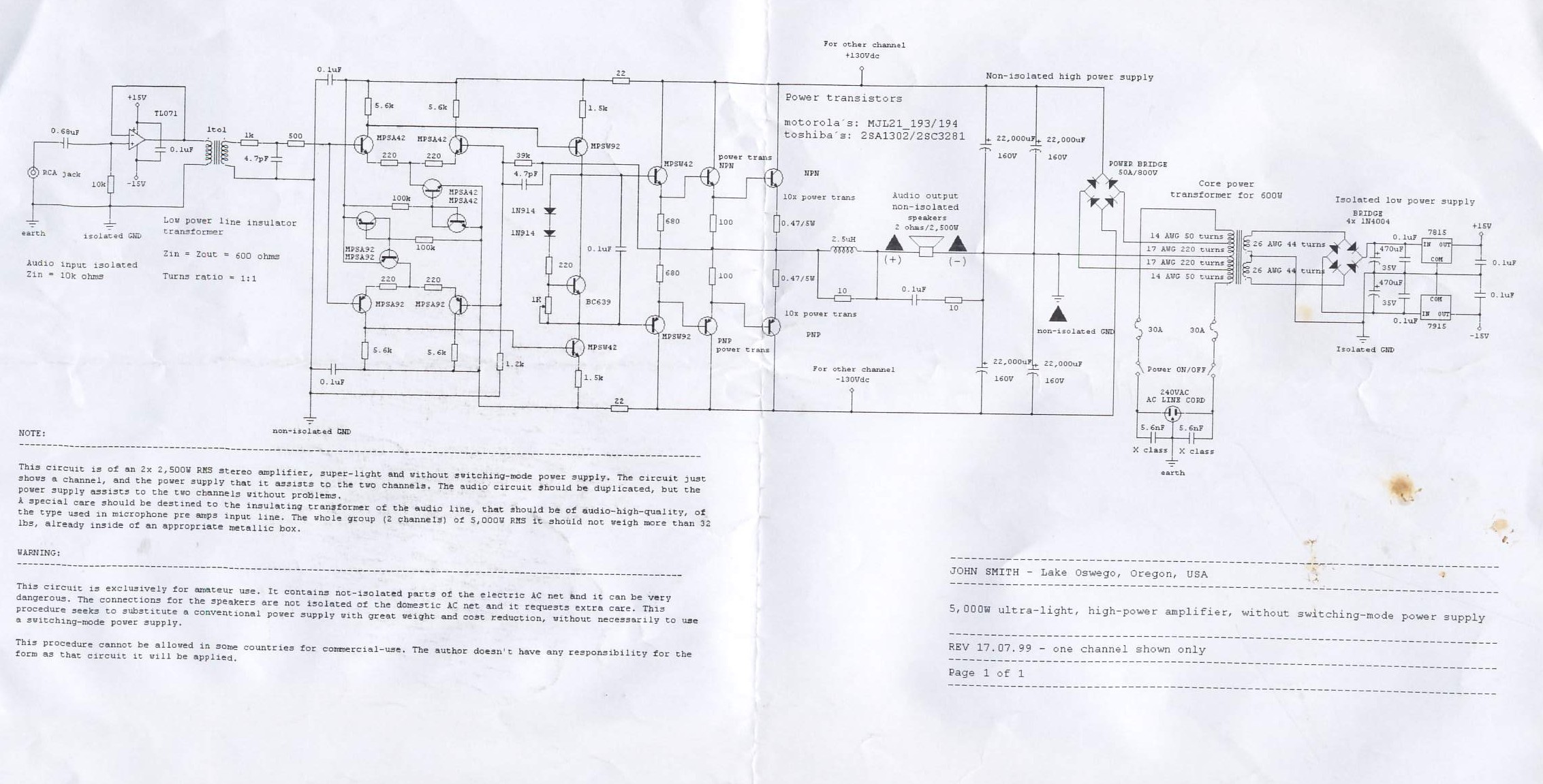
This circuit is for a 2x2, 500W RMS stereo amplifier that is super-light and does not utilize a switching-mode power supply. The circuit diagram displays only one channel, while the power supply is designed to support both channels. The...
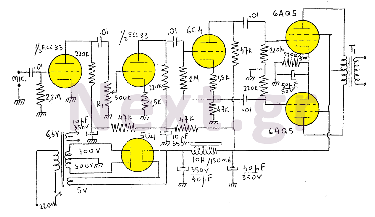
The output of this modulator consists of two 6AQ5 lamps arranged in a push-pull configuration with a maximum output of 15W. A 6C4 lamp is employed as a reversing lamp. The double-stage ESC83 serves as the pre-amplifier. The potentiometer...
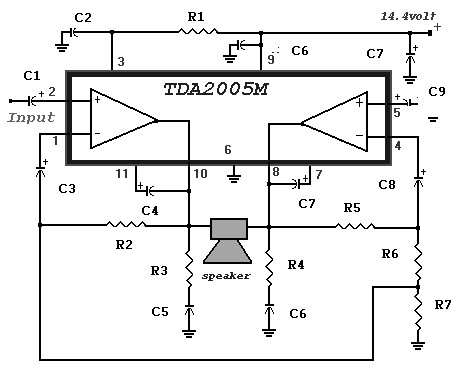
A 20 Watt car power amplifier circuit diagram based on the TDA 2005. The TDA 2005 IC is specifically designed for power boosting applications in car audio systems. This IC includes protection against short circuits and overheating. The circuit...
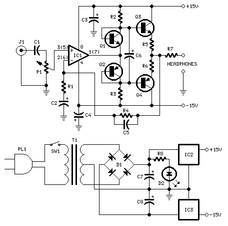
High Quality unit with LM833 or NE5532 Low noise Dual Op-amp. No need for a preamplifier. Can be directly connected to CD players, tuners and tape recorders. Tested with several headphone models of different impedance: 32, 100, 245, 300,...
The LM231 and LM331 family of voltage-to-frequency converters are well-suited for use in simple, low-cost circuits designed for analog-to-digital conversion, precision frequency-to-voltage conversion, long-term integration, linear frequency modulation or demodulation, and various other applications. When utilized as a voltage-to-frequency...
This structure is a radio frequency (RF) amplifier designed for small UHF TV transmitters, operating within the UHF channel range of 450-800 MHz. The amplifier enhances video signals in this frequency range and operates in Class A, utilizing the...