
20Khz-arc-welding-inverter
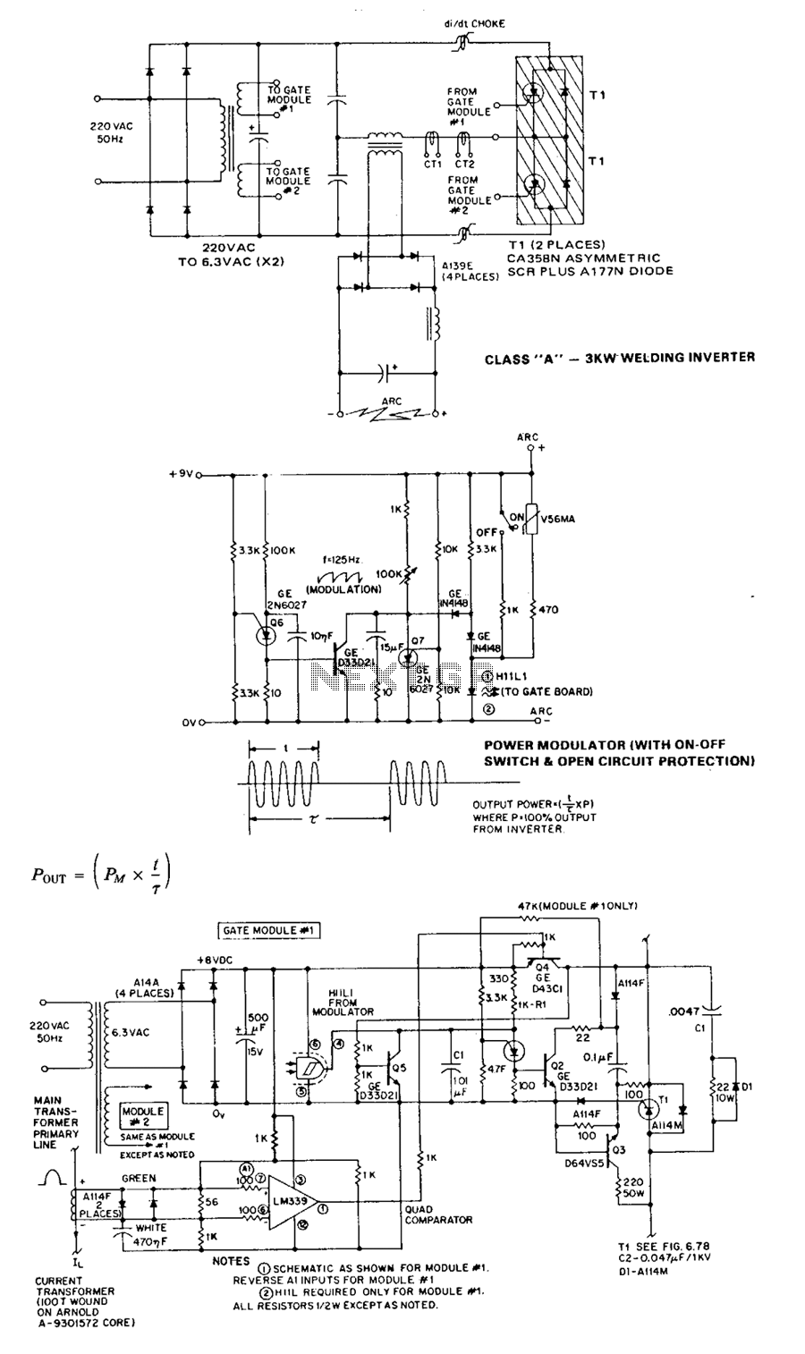
The circuit operates without significant added complexity and has a natural tendency to run away under no-load (high Q) conditions. The 20-kHz control circuit addresses these issues by feeding back into the asymmetrical thyristor trigger pulse generators signals that simultaneously shut down the inverter when its output voltage exceeds a preset threshold, followed by time-ratio modulation of the output. This feedback is achieved with full galvanic isolation between input and output, utilizing an opto-Schmitt coupler. The fundamental 20-kHz gate firing pulses are generated by a PUT relaxation oscillator. These pulses are then amplified by transistors. The 20-kHz sinusoidal load current flowing in the primary of the output transformer is detected by a current transformer, with an operational amplifier converting the sine wave into a square wave, whose transitions align with the load current zero points. Each time the output current changes, the operational amplifier also changes state and, through a transistor, either connects the thyristor gate to a -8 V DC supply for minimum gate-assisted turn-off time and maximum reapplied dV/dt capability or disables this supply to prepare the thyristor for subsequent firing. Modulation intelligence is fed into the opto-Schmitt coupler through two additional PUTs, one of which oscillates at a fixed frequency, establishing the modulation frequency. The duty cycle is determined by a second oscillator, whose conduction state controls current to the opto-Schmitt coupler diode. The inverter operates at a fundamental frequency of 20 kHz with a modulation frequency of 1.25 kHz. When the output power is at maximum, it is 100% continuous, while the minimum power is one cycle of 20 kHz (50 µs) within the 1.25 kHz modulation frame (800 µs), resulting in 6.25% of maximum power.
The described circuit is a sophisticated control system for an inverter, employing a 20-kHz control circuit designed to manage the output voltage effectively. The circuit's architecture includes a feedback mechanism that leverages an opto-Schmitt coupler to ensure isolation between the control and power sections, which is critical for safety and performance. The use of a PUT relaxation oscillator to generate the gate firing pulses indicates a design choice aimed at achieving precise timing for the thyristor operation, essential for maintaining the desired output characteristics.
The current transformer plays a crucial role in monitoring the load current, enabling the operational amplifier to convert the detected sinusoidal waveform into a square wave. This transformation is significant as it allows for real-time monitoring of the load current's zero crossings, facilitating timely adjustments to the thyristor gate control. The switching behavior of the operational amplifier, in response to load current changes, is instrumental in managing the thyristor's conduction state, thus optimizing the inverter's performance.
The modulation scheme, which involves two additional PUTs for establishing a modulation frequency of 1.25 kHz, enhances the system's versatility. This modulation frequency allows for dynamic adjustments to the output power, ensuring efficient operation under varying load conditions. The duty cycle management through the second oscillator provides further control over the output characteristics, allowing the inverter to adapt to different operational requirements.
Overall, the circuit's design demonstrates an effective integration of feedback control, isolation techniques, and modulation strategies, resulting in a robust inverter system capable of maintaining stable output across a range of conditions while minimizing the risks associated with high-Q behavior.without significant added complexity, and a natural tendency to run away under no-load (high Q) conditions. The 20-kHz control circuit (see Fig. 2) overcomes these shortcomings hy feeding back into the asymmetrical thyristor trigger pulse generators (see Fig.
3) signals that simultaneously shut the inverter down, when its output voltage exceeds a preset threshold, then time-ratio modulates the output. This feedback is accomplished with full galvanic isolation between input and output thanks to an HllL opto-Schmitt coupler.
The fundamental 20-kHz gate firing pulses are generated by a PUT relaxation oscillator Ql. The pulses are then amplified by transistors Q2 and Q3. The 20-kHz sinusoidal load current flowing in the primary of the output transformer is then detected hy current transformer CTl, with op amp Al converting the sine wave into a square wave, whose transitions coincide with the load current zero points. Consequently, each time the output current changes, phase Al also changes state and, via transistor Q4, either connects the thyristor gate to a -8 V de supply for minimum gate assisted tnm-off time and highest reapplied dV/dt capability or disables this supply to prepare the thyristor for subsequent firiog.
Modulation intelligence is coupled into this same HllL through two additional PUTs, Q6 and Q7, Q6 oscillates at a fixed 1.25 kHz, which establishes the modulation frequency. The duty cycle is determined by a second oscillator, Q7, whose conduction state, on or off, establishes or removes current from the HllL diode.
With a fundamental inverter frequency of 20kHz and a modulation frequency of 1.25 kHz. Where PM ~ 100% continuous output power. Minimum power is one cycle of 20kHz (50 p.s) in the 1.25- kHz modulation frame (800 p.s), that is, 6.25% PM. 🔗 External reference
Related Circuits

The Class A series resonant inverter is recognized for its high efficiency, low cost, and compact size, provided the operating frequency exceeds approximately 3 kHz. However, it faces challenges, particularly in high power versions, regarding the difficulty of achieving...