
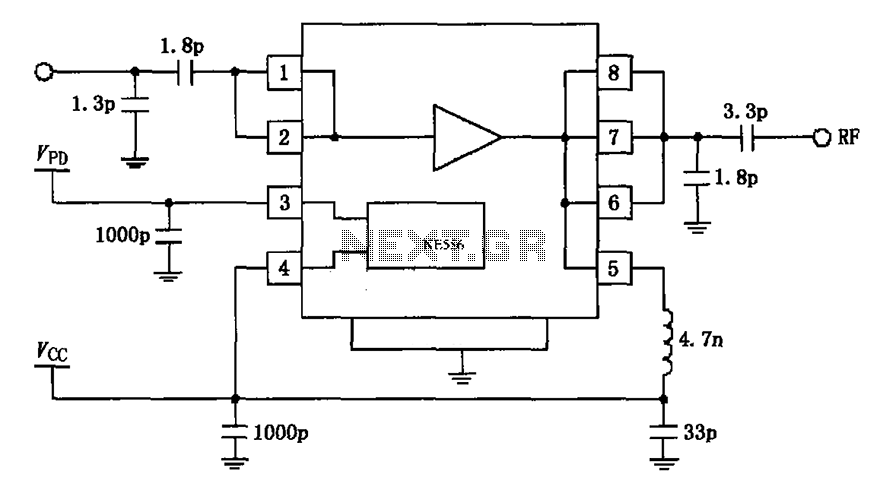
2450MHz end-stage linear power amplifier configuration of the circuit diagram RF2126
The RF2126 is designed for applications that demand high linearity and efficiency in the amplification of RF signals. The device operates within the 2.4 GHz ISM band, making it suitable for various wireless communication protocols. The amplifier's architecture typically includes multiple gain stages, enhancing signal strength while maintaining signal integrity.
The input stage, connected to pin 1, is critical for ensuring optimal signal transfer from the source to the amplifier. The blocking coupling capacitor serves to prevent DC voltage from affecting the signal path, thereby protecting the subsequent amplifier stages. The choice of a capacitor value between 1.8 µF and 2.0 µF is essential for matching the input impedance to the characteristic impedance of the RF signal, which is standardized at 50 ohms in many RF applications.
The output stages of the RF2126, represented by pins 5, 6, and 8, are designed to deliver the amplified RF signal to the load while minimizing distortion. The circuit layout should consider the transmission line effects and impedance matching to ensure maximum power transfer and minimize signal reflections. Proper grounding and decoupling techniques are also vital in maintaining the performance of the amplifier, especially at high frequencies.
In summary, the RF2126 amplifier circuit is a sophisticated design suitable for high-frequency applications, with careful attention paid to component selection and circuit layout to achieve reliable and efficient RF signal amplification. As shown in FIG constituted by RF2126 2450MHz end-stage linear power amplifier circuit. Radio frequency (RF) signal from the input pin 1, after amplified by the amplifier 7 fee t (5,6,8) output. Pin 1 is directly coupled to the internal amplifier, so a foot plus a blocking coupling capacitor. Blocking coupling capacitor has a capacity of 1.8 ~ 2.0 F, 1 foot input impedance of 50. Figure capacitance and inductance values are typical values 2450MHz frequency when.
Related Circuits
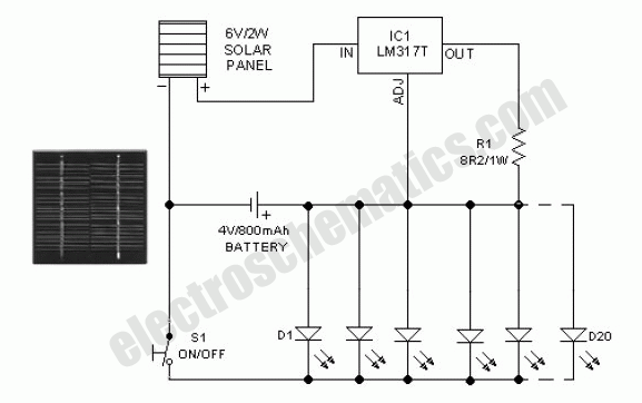
This Outdoor LED Solar Garden Lights project is a hobby circuit for an automatic garden light that utilizes a light-dependent resistor (LDR) and a 6V/5W solar panel. During daytime, the internal rechargeable 6 Volt sealed lead-acid (SLA) battery is...
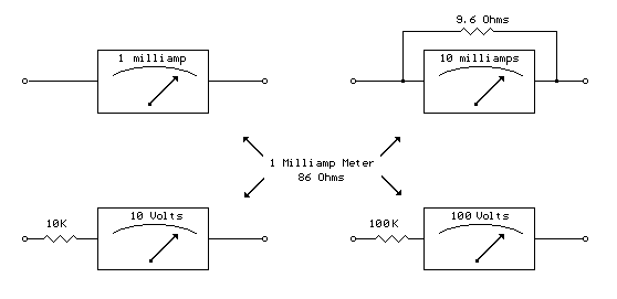
A milliamp meter can function as a voltmeter by incorporating a series resistance. The required resistance is calculated by dividing the full-scale voltage reading by the full-scale current of the meter movement. For instance, using a 1 milliamp meter...
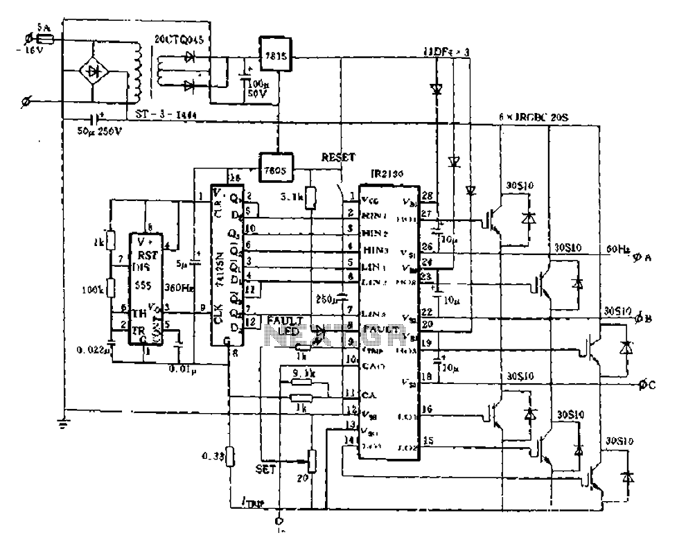
The application of the aforementioned advantages allows the IR2130 to be effectively utilized for DC cut crossing speed, DC servo systems, three-phase power inverters, and switching power supplies. Additionally, it is applicable in inverter power supplies, uninterruptible power supplies...
The IR Theremin hardware schematic is notably simple, as the primary input and output devices require minimal connections. This simplicity can be a double-edged sword, as fewer hardware components often lead to increased software complexity. The main components utilized...

This class of amplifier is designed to follow low-level stages, such as a crystal oscillator. An oscillator requires an intermediate stage to prevent loading, ensuring that the input impedance is sufficiently high to avoid significant loading on the oscillator....
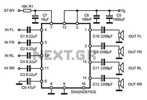
The following circuit illustrates a 35W quadruple amplifier and a 2 x 25W bridge amplifier based on the TDA7375 integrated circuit (IC). This circuit requires a minimal number of external components. Although initially designed for car applications, it can...