
buffer amplifiers

Buffer amplifiers serve as critical components in electronic circuits, particularly for applications requiring impedance matching and signal integrity. In a typical configuration, the buffer amplifier receives a low-level signal from a source, such as a crystal oscillator. The buffer's high input impedance ensures that it does not load the oscillator, preserving the oscillator's performance and frequency stability. The output stage of the buffer amplifier is designed to drive the next component in the signal chain, which may include mixers, filters, or amplifiers.
In the case of a voltage-controlled oscillator (VCO) operating at 1.8 to 2.0 MHz, the buffer amplifier plays a crucial role in isolating the oscillator from subsequent stages while providing sufficient drive capability. The choice between FET and bipolar transistors hinges on the specific application requirements and available components. FETs, with their high input impedance, are particularly advantageous when interfacing with high-impedance sources, while bipolar transistors offer robust performance in various applications.
The calculations related to power gain and voltage levels illustrate the importance of understanding the relationships between voltage, impedance, and power in circuit design. For instance, using the formula P = E² / R allows designers to quantify the power available to subsequent stages, ensuring that the system functions efficiently without introducing distortion or other undesirable effects. The ability to achieve significant power gain while maintaining a manageable voltage output is a key design consideration for buffer amplifiers in various electronic applications.This class of amplifier is designed to follow low level stages, one example is a crystal oscillator. An oscillator for optimum performance can NOT be loaded down, it needs an intermediate stage following. This will then present a sufficiently high enough input impedance so it is not considered a significant load to the oscillator.
The intermediate or buffer stage, while not representing a load must then have a sufficiently low output impedance to drive successive stages. If these concepts of impedance confuse or worry you then look at my other page " what is impedance " it`s a rough and ready explanation, followed by a more technical explanation of impedance matching but hopefully you will come back with a considerably better understanding.
From what I said above, two desirable traits of a buffer amplifier are high input impedance and low output impedance. Obviously succeeding stages should also be linear because we don`t want to introduce distortion. As a matter of interest a buffer amplifier is not solely limited to following an oscillator. You could have a requirement of wanting to sample the output of the first mixer for what is called a "Panadaptor", a means of visually seeing adjacent signals on an oscilloscope.
Also a high quality agc system should be derived from the last i. f. stage, it should be buffered before going to the agc amplifier and then on to the agc detector. Other examples are low level outputs of audio amplifier stages such as microphone inputs where the microphone is a high impedance type. Although not so common now, phono inputs to audio ampliers also needed buffering. Here I`m going to use a very practical example where one of my readers has a requirement for a voltage controlled oscillator operating at 1.
8 - 2. 0 Mhz (amateur radio band 160M). This is to be part of a frequency synthesiser. We can look at two types of active devices for use in buffer amplifiers, FET transistors and bipolar transistors. Choice is largely a matter of opinion but more often it depends on what you have on hand. Bipolar types are referred to as "emitter followers". Now it is considered bad practice to use the output of the oscillator to drive succeeding stages because in loading down the oscillator we cause frequency pulling and a host of other unwanted maladies.
That`s about as basic as it gets. The FET represents a high input impedance (Z) but a relatively low output impedance. This buffer amplifier configuration, called a "source follower", is capable of high power gain, perhaps as much as 25 db BUT the voltage output would be only around 90% of the input which is a voltage gain of -0. 5 dB (loss) Confused. Look at it this way - consider an input signal of say 50 mV RMS. I`ve just said the output voltage is about 90% or in this case 45 mV, yet I spoke of Power Gain, in fact 25 dB perhaps.
Assume for purposes of discussion only, that the input impedance is 100K or 100, 000 ohms. If the output power available to the succeeding stage is assumed to be sourced from a relatively low 270 ohms source, albeit at a reduced voltage of 45 mV RMS, then our calculations are P = E2 / R or [ ( 0. 045V * 0. 045V ) / 270 this equals 7. 5 micro-watts. It further follows that for 7. 5 uW output after a 0. 025 uW input there must have been a power gain of 7. 5 / 0. 025 = 300 which 10 * log (300) = 24. 77 or say 25 dB. 🔗 External reference
Related Circuits
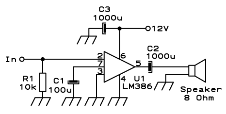
Approximately one watt RMS appears to be a suitable output level, which is also the maximum power that a basic amplifier powered by 12V can deliver to an 8 Ohm speaker. A very low saturation amplifier may reach up...
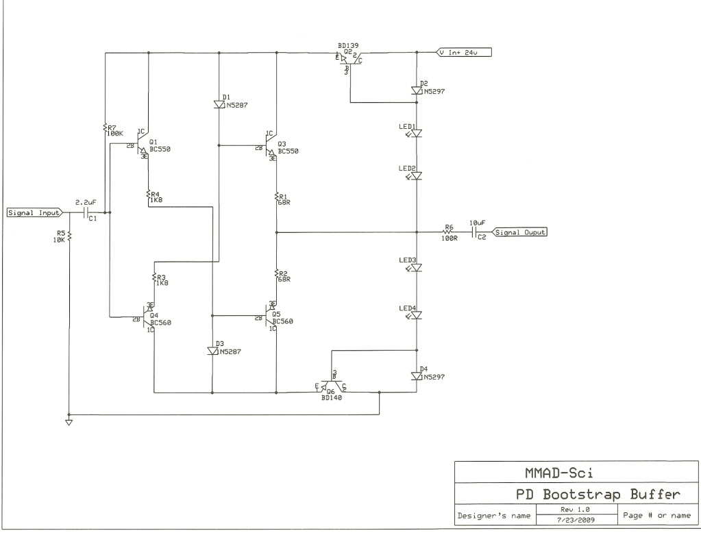
Various circuit variations have been explored, including a standalone preamp, headphone amplifier, replacements for the 321/729 circuits, and a potential active crossover, depending on demand. There has been significant interest in these designs, and the bootstrap buffer preamp is...
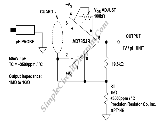
A buffer amplifier is necessary for a typical pH probe to isolate its source resistance, which ranges from 10^6 to 10^9 ohms, from the external circuitry. Such an amplifier is illustrated in the... The buffer amplifier serves a critical role...
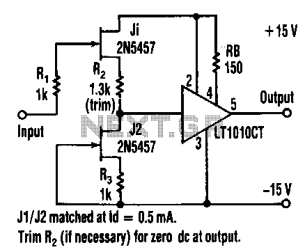
This buffer amplifier's overall harmonic distortion is low at 0.01% or less at a 3-V RMS output into a 500-ohm load without overall feedback. The LT1010CT features a slew rate of 100 V/µs, a video bandwidth of 20 MHz,...
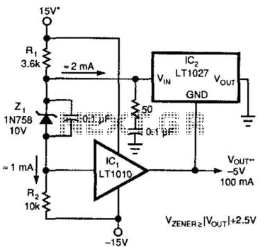
A method for enhancing the output current of a reference while also providing overload protection is illustrated. In this configuration, IC1 functions as a power buffer. The LT1027 regulates the output voltage (Vout) and ground to maintain a stable...
An audio power amplifier can enhance weak signals from devices like tuners, CD players, or tape decks to fill a room with sound. This article emphasizes the operating principles and circuitry of low-frequency power amplifiers utilizing bipolar junction transistors...
Warning: include(partials/cookie-banner.php): Failed to open stream: Permission denied in /var/www/html/nextgr/view-circuit.php on line 713
Warning: include(): Failed opening 'partials/cookie-banner.php' for inclusion (include_path='.:/usr/share/php') in /var/www/html/nextgr/view-circuit.php on line 713