3-Wire Receiver/Message Demuxer

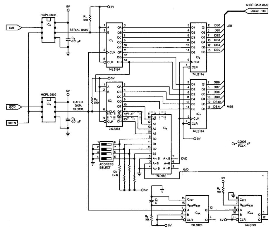
This 3-wire receiver verifies the initial four data bits of 16 received bits against a predetermined address. If the two match, the remaining 12 bits are stored in two 6-bit flip-flop registers. The design can utilize either CMOS or TTL logic families.
The described circuit functions as a data receiver that compares incoming data against a specified address. It operates with a three-wire interface, which typically includes a data line, a clock line, and a control line. When 16 bits of data are received, the first four bits are extracted for comparison with a preset address stored in the circuit.
If the first four bits match the preset address, the circuit proceeds to latch the remaining 12 bits into two separate 6-bit flip-flop registers. These flip-flops serve as temporary storage elements, allowing the system to hold the data for further processing or output. The use of flip-flops ensures that the data remains stable and can be accessed reliably after the initial data reception.
The choice between CMOS and TTL logic families provides flexibility in design, allowing engineers to select components based on power consumption, speed, and integration requirements. CMOS technology typically offers lower power consumption and higher noise immunity, making it suitable for battery-powered applications. In contrast, TTL may be preferred in high-speed applications due to its faster switching times.
Overall, this 3-wire receiver circuit is versatile and can be adapted to various applications requiring data verification and storage. This 3-wire receiver checks the first four data bits of 16 received bits against a preset address. If the t wo match, the remaining 12 bits are latched into two 6-bit flip-flop registers. Either CMOS or TTL logic families can be used in the design.
