
3-Wire Serial LCD using PIC12F683

- Initialize_LCD(): It initializes the LCD module to operate into 4-bit mode, 2 lines display, 5x7 size character, display ON, and no cursor.
- Write_LCD_Data(): Sends a character byte to display at current cursor position.
- Write_LCD_Cmd(): Write a command byte to the LCD module.
- Write_LCD_Nibble(): Data or command byte is sent to the LCD module as two nibbles. So this function routine takes care for sending the nibble data to the LCD module.
- Write_LCD_Text(): This routine is for sending a character string to display at current cursor position.
- Position_LCD(): To change the current cursor position.
At the beginning of your program, you need to define Data_Pin, Clk_Pin, and Enable_Pin to the chosen microcontroller ports. I am going to demonstrate here how to use these driver routines to display two blinking character strings, Message1 and Message2, at different locations. I am going to test our serial LCD module with PIC12F683 microcontroller. The test circuit is shown below.
Note: PIC12F683 Settings
Running at 4 MHz internal clock, MCLR disabled, WDT OFF.
Clock, Data, and Enable lines are served through GP1, GP5, and GP2 ports.
The circuit employs a 74HC595 shift register to facilitate the communication between the microcontroller and the LCD. The microcontroller sends serial data to the DS pin of the shift register, which is configured to output parallel data to the LCD. The shift register's SH_CP and ST_CP clocks are tied together, ensuring that data is shifted into the register on the rising edge of the clock. This configuration requires careful timing, as an additional clock pulse is needed to synchronize the output of the storage register with the shift register.
The LCD operates in 4-bit mode, necessitating the transmission of data in two nibbles. The microcontroller communicates with the shift register using two pins for clock and data, while a third pin is utilized for enabling the LCD. The R/W pin of the LCD is grounded, indicating that it will only receive data and commands, not send any status back to the microcontroller.
Initialization routines must be executed to set the LCD into the correct mode. The driver functions facilitate the sending of commands and data to the LCD, allowing for the display of text strings at designated cursor positions. The implementation of these routines in the mikroC compiler ensures compatibility with a 16x2 LCD module, though adjustments can be made for different configurations. The test setup with the PIC12F683 microcontroller demonstrates the practical application of this circuit design. The character data and command from the microcontroller is transferred serially to a shift register (74HC595), and the parallel output from the shift register is fed to LCD pins. 74HC595 is a high-speed 8-bit serial in, serial or parallel-out shift register with a storage register and 3-state outputs.
The shift register and storage registers have separate clocks, SH_CP and ST_CP respectively. Data in the shift register is shifted on the positive-going transitions of SH_CP, and the content of shift register will be transferred to the storage register on a positive-going transition of the ST_CP. If we tie both the clocks together, the shift register will always be one clock ahead of the storage register.
The 8-bit data of the storage register will appear at the parallel output (Q0-Q7) when the output enable (OE) is low. In this project, SH_CP and ST_CP are tied together. So, if we want to receive a serially transferred 8-bit into parallel form at Q0-Q7, an extra clock pulse is required after transmitting the 8-th bit of serial data because the clocks are tied and the storage register is 1-clock behind the shift register. The hardware part of this project is fairly simple. The challenging part is to write the driver software that is responsible for a proper sequence of operations required to serially transfer character data and command to 74HC595 serial-in parallel-out shift register.
The shift register parallel output is then connected to LCD data lines (D4-D7) and RS control pin. This arrangement requires 3-pins of microcontroller to display character data on a parallel LCD display: 2 pins for providing Clock and Data to 74HC595, and 1 pin for enable control (E) pin of LCD module. Since the data transfer uses 4-bit mode, any 8-bit command or character data is sent in two steps: send the higher nibble first, and then the lower nibble.
The R/W control pin is grounded, and therefore no data or status read from the LCD module is possible in this case. A first, a bit of data fed to DS pin of 74HC595 appears at Q0 output after 2 clocks (because SH_CP and ST_CP are tied).
So, sending 4-bit data (D4-D7) and an RS signal require 6 clock pulses till they appear at Q0-Q4 outputs respectively. When the LCD module is turned ON, it is initialized in 8-bit mode. A number of initializing commands should be sent to operate the LCD module in 4-bit mode. All the driver routines that are discussed here are written in mikroC compiler. They work only for a 16x2 LCD module. User can modify the initialization operations inside the Initialize_LCD() routine to account for other LCD configurations.
The driver routines and their functions are described below. - Initialize_LCD() : It initializes the LCD module to operate into 4-bit mode, 2 lines display, 5x7 size character, display ON, and no cursor. - Write_LCD_Data() : Sends a character byte to display at current cursor position. - Write_LCD_Cmd() : Write a command byte to the LCD module. - Write_LCD_Nibble() : Data or command byte is sent to the LCD module as two nibbles. So this function routine takes care for sending the nibble data to the LCD module. - Write_LCD_Text() : This routine is for sending a character string to display at current cursor position.
- Position_LCD() : To change the current cursor position At the beginning of your program, you need to define Data_Pin, Clk_Pin, and Enable_Pin to the chosen microcontroller ports. I am going to demonstrate here how to use these driver routines to display two blinking character strings, Message1 and Message2, at different locations.
I am going to test our serial LCD module with PIC12F683 microcontroller. The test circuit is shown below. Note: My PIC12F683 Settings Running at 4 MHz internal clock, MCLR disabled, WDT OFF. Clock, Data, and Enable lines are served through GP1, GP5, and GP2 ports. 🔗 External reference
Related Circuits
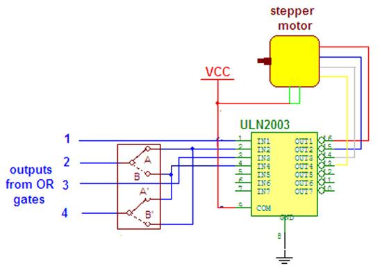
Wireless stepper motor speed control project using a laser and IC555. This project provides insights into the fundamentals and circuit construction for controlling the speed of a wireless stepper motor utilizing a laser and the IC 555 timer. The project...
The enable signal for the USB chip and GLCD controller is generated by a PLD decoder from the address lines. The memory map for the I/O of the 8051SBC board indicates that the available space ranges from 0x0300 to...
A 25kHz thyristor inverter welding machine circuit utilizes high-frequency operation to enable smaller transformer designs. The circuit diagram is illustrated in Figure 9-14. The no-load output voltage of the machine is 45V DC, with a peak voltage of 90V...
Telephone ringer utilizing 556 dual timers. This circuit generates ringing tones resembling those of a telephone by employing modulated rectangular waves of varying time periods. The telephone ringer circuit employs two 556 dual timer ICs configured to generate modulated rectangular...
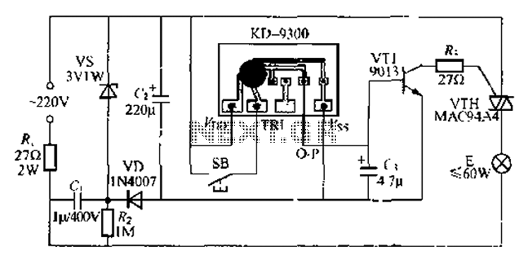
The circuit utilizes a KD-9300 music IC, which activates when the button switch (SB) is pressed, causing the electric lamp (E) to light up for approximately 20 seconds before automatically turning off. The setup includes a half-wave rectifier and...
How can a television modulator be small and simple? First, it utilizes integrated circuits, and second, a TV modulator is essentially an amplitude modulator. Television modulators are essential components in the transmission of television signals, converting audio and video signals...