
8-bit Digital to Analog converter (DAC)
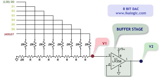
The digital-to-analog converter (DAC) based on the R/2R resistor network is a fundamental and effective way to convert digital signals into analog voltages. The operation of the R/2R network relies on the precise arrangement of resistors, where each branch of the network contributes to the final output voltage based on the binary input values. The key to ensuring accuracy in the output voltage lies in the resistor values, which should closely adhere to the R/2R ratio.
In practical applications, the construction of the DAC requires careful attention to the layout and connections to minimize noise and interference. The op-amp used in the voltage buffer stage must be selected based on its specifications, particularly its output voltage range and linearity characteristics. Proper decoupling capacitors should be employed near the power supply pins of the op-amp to stabilize the supply voltage and reduce the impact of transient load changes.
To enhance performance, additional components such as low-pass filters may be implemented at the output to smooth out any high-frequency noise that may be present due to the rapid switching of the digital inputs. The design should also account for the input impedance of the subsequent stages to ensure that the voltage buffer effectively isolates the DAC output from any loading effects.
Overall, the R/2R DAC, when properly designed and implemented, provides a reliable means of converting digital signals to analog voltages for various applications, including audio processing, signal generation, and control systems. By understanding the principles behind the R/2R network and the importance of the voltage buffer, one can successfully construct a functional and accurate DAC.This article aims to introduce to beginners and intermediate readers a simple solution to build a digital to analog converter, based on the famous r/2r resistors network. This article also discuss a problem encountered by many beginners while trying to build their own DAC, and proposes some very simple solutions to that problem.
Through this artic le, I am going to explain how to build an 8-bit digital to analog converter with parallel input. If you don`t know what this means, well its simply a circuit that will take as input a digital 8-bit number from 0 (00000000) to 255 (11111111), and output the relative value on a scale from 0 to 5v. Then the output voltage for the converter should be equal to the binary input multiplied by the step value, e.
g. for an input of 129 (1000 0001 in binary) the output voltage should be: The digital data entering thought the 8 lines (D0 to D7) are going to be converted to an equivalent analog voltage (Vout) by the mean of the R/2R resistor network. Actually a lot of commercial Digital to Analog converter ICs are based on this same principle. The R/2R network is build by a set of resistors of two values, with one of them double the other (example 10K and 20K), in on of my circuits I used 1M ohm and 470K ohm resistors, which is quite near to the R/2R ratio, and this small difference didn`t cause any detectableerrors in most applications.
However, if you want to build a very precise DAC, be precise when choosing the values of the resistors that will exactly match the R/2R ratio. Note that you can build a DAC with any number of bits you want, simply by enlarging the resistor network, by adding more R/2R branches (like the one shaded in green), BUT you must keep the 2R resistance connected to ground (shaded in light red) Now, in order to use this Resistor Network (also called R/2R Ladder) for real applications, you will have to build a very simple voltage buffer circuit, which will be explained in the next section.
All the components are labeled on the circuit, so i`ll start directly to explain how it works. To simplify this task, i`ll split the circuit into two main stages: the Digital to analog converter and the Voltage buffer stage. This part have been explained in detail in the previous section, its purpose is to create the voltage V1 which is equivalent to the weight of the binary number on the lines (D0toD7).
Now that this is a resistor network, if we apply any load on the output of the first stage, this load will be considered as an additional resistor in the network, and thus will disturb the network which will no longer provide the correct & desired output voltage. Therefore, to overcome this problem, we need a voltage buffer, here is where the next stage comes This stage will isolate the point V1 from the final output V2, while always keeping the voltage V2 at the exact same value of V1.
This is what we call a voltage buffer. for the voltage buffer we use an opamp with the output connected to the inverting input (this special configuration of the Op Amp is also called Voltage Follower). The most important things to note are: A quick look on those two graphs can be sufficient to understand the problem: the output of the op-amp is not linear on the full 0-to-Vcc scale.
actually an OpAmp, depending on its type, will deliver a maximum voltage of (Vcc 0. 5V), where Vcc is the supply voltage of the OpAmp. So, in our application, the OpAmp will only deliver 4. 5V even if theoretically it should deliver 5V. Lets get a little deeper into the problem, the actual output curve in red should be linear, but actually it begins loosing its linearity beginning from 3. 9 volt. (Again this depends on the type of OpAmp, those results a based on my own tests on a LM350 OpAmp) The red Error zone` is where the output of the DAC no longer math the relative binary input.
The first solutions shown in the red shading is to increase the supply voltage o 🔗 External reference
Related Circuits
A digital amplifier is a new device that IC manufacturers are eager to capitalize on, leading to the launch of unique digital amplifier products. Below are brief descriptions of some representative devices. The TA2022, produced by Tripath, is an...
This project is an audio amplifier designed to amplify output signals from small radios, tape players, CD players, or other audio signal sources. For stereo operation, two identical amplifiers must be constructed—one for the left channel and another for...
This is a video scan converter to display NTSC video signal into VGA monitor. Normally, the VGA monitor occupies most desk top space, so that everybody will be thinking that if the VGA monitor can be used for video...
The M-8880 is a complete DTMF Transmitter/Receiver that features adjustable guard time, automatic tone burst mode, call progress mode, and a fully compatible 6500/6800 microprocessor interface. The receiver portion is based on the industry-standard M-8870 DTMF Receiver, while the...
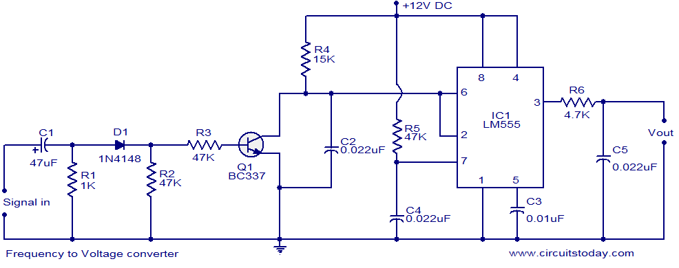
A simple frequency to voltage (F to V) converter circuit utilizing the LM555 Timer IC. This circuit has numerous applications in digital frequency meters, tachometers, and other related devices. The frequency to voltage (F to V) converter is a crucial...
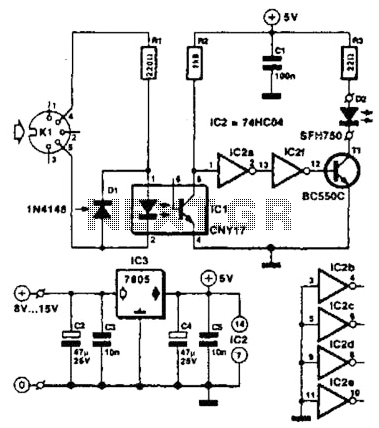
Used for digital control of musical instruments, this transmitter converts digital data signals into equivalent optical signals for a fiber optic cable interface. Optocoupler IC1 provides isolation, driving IC2-a and -b, and T1, ultimately providing a cable driver LED...