
Class B audio amplifier Analog Integrated Circuits
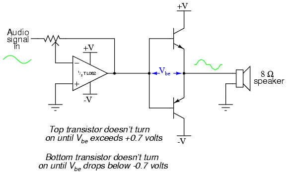
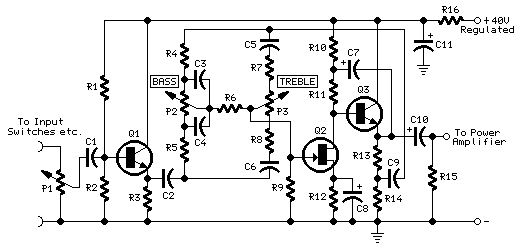
The audio amplifier circuit described operates using a class B push-pull configuration, which is favored for its efficiency in power amplification. Each transistor in the circuit is responsible for driving the load during alternate half-cycles of the input signal, preventing continuous conduction and thus reducing thermal stress. The design allows for a straightforward connection to various audio sources, facilitating versatility in application.
The operational amplifier included in the circuit serves a critical role in managing the transition between the two output transistors. By implementing negative feedback, it effectively minimizes the crossover distortion typically associated with class B amplifiers, enhancing overall sound quality. This is particularly important in audio applications where fidelity is paramount.
The circuit's layout should include appropriate biasing resistors to set the operating point of the transistors, ensuring that they remain in the desired mode of operation. The use of capacitors for coupling and decoupling signals is also essential to maintain signal integrity and prevent unwanted noise from affecting performance.
In practical terms, careful consideration must be given to the selection of transistors, as their characteristics directly influence the amplifier's performance. Additionally, the choice of power supply voltage will impact the output power and headroom available for the amplifier. Experimentation with different speaker loads and configurations can further optimize the amplifier's performance, tailoring it to specific audio applications.This project is an audio amplifier suitable for amplifying the output signal from a small radio, tape player, CD player, or any other source of audio signals. For stereo operation, two identical amplifiers must be built, one for the left channel and other for the right channel.
To obtain an input signal for this amplifier to amplify, just connect it to the output of a radio or other audio device like this: This amplifier circuit also works well in amplifying "line-level" audio signals from high-quality, modular stereo components. It provides a surprising amount of sound power when played through a large speaker, and may be run without heat sinks on the transistors (though you should experiment with it a bit before deciding to forego heat sinks, as the power dissipation varies according to the type of speaker used).
The goal of any amplifier circuit is to reproduce the input waveshape as accurately as possible. Perfect reproduction is impossible, of course, and any differences between the output and input waveshapes is known as distortion. In an audio amplifier, distortion may cause unpleasant tones to be superimposed on the true sound. There are many different configurations of audio amplifier circuitry, each with its own advantages and disadvantages.
This particular circuit is called a "class B, " push-pull circuit. Most audio "power" amplifiers use a class B configuration, where one transistor provides power to the load during one-half of the waveform cycle (it pushes) and a second transistor provides power to the load for the other half of the cycle (it pulls). In this scheme, neither transistor remains "on" for the entire cycle, giving each one a time to "rest" and cool during the waveform cycle.
This makes for a power-efficient amplifier circuit, but leads to a distinct type of nonlinearity known as "crossover distortion. " If the "hand-off" between the two transistors is not precisely synchronized, though, the amplifier`s output waveform may look something like this instead of a pure sine wave: Here, distortion results from the fact that there is a delay between the time one transistor turns off and the other transistor turns on.
This type of distortion, where the waveform "flattens" at the crossover point between positive and negative half-cycles, is called crossover distortion. One common method of mitigating crossover distortion is to bias the transistors so that their turn-on/turn-off points actually overlap, so that both transistors are in a state of conduction for a brief moment during the crossover period: This form of amplification is technically known as class AB rather than class B, because each transistor is "on" for more than 50% of the time during a complete waveform cycle.
The disadvantage to doing this, though, is increased power consumption of the amplifier circuit, because during the moments of time where both transistors are conducting, there is current conducted through the transistors that is not going through the load, but is merely being "shorted" from one power supply rail to the other (from -V to +V). Not only is this a waste of energy, but it dissipates more heat energy in the transistors. When transistors increase in temperature, their characteristics change (Vbe forward voltage drop, ², junction resistances, etc.
), making proper biasing difficult. In this experiment, the transistors operate in pure class B mode. That is, they are never conducting at the same time. This saves energy and decreases heat dissipation, but lends itself to crossover distortion. The solution taken in this circuit is to use an op-amp with negative feedback to quickly drive the transistors through the "dead" zone producing crossover distortion and reduce the amount of "flattening" of the waveform during crossover. The first (leftmost) op-amp shown in the schematic diagram is nothing more than a buffer. A buffer helps to reduce the loading of the input capac 🔗 External reference
Related Circuits
A meter is a device designed to accurately detect and display an electrical quantity in a form that is readable by humans. This "readable form" is typically visual, such as the motion of a pointer on a scale, a...
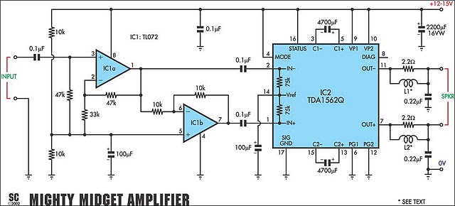
It is based on a Philips class-H audio amplifier integrated circuit and can deliver 36W RMS or 70W music power, all from a 13.8V supply. The new Mighty Midget Amplifier can produce approximately 36W RMS continuously into a 4-ohm...
Although there is a need for an integrated circuit (IC), the interface between the modulator and audio-video signals has not yet been developed as an IC. This is primarily due to the complexity of such a design, the variations...
R1 2.2K 1/4W Resistor, R2 27K 1/4W Resistor, R3, R4 2.2K 1/2W Trimmers (Cermet or Carbon), R5 100R 1/4W Resistor, R6 1K 1/4W Resistor, R7, R8 330R 1/4W Resistors, C1 22 µF 25V Electrolytic Capacitor, C2 47pF 63V Polystyrene...

This notch filter is beneficial for tunable band-reject applications in the audio range. The specified values will provide a tuning range of approximately 300 to 1500 Hz. The notch filter is designed to attenuate a specific frequency while allowing others...
A unit that is often very useful for isolating two stages in sound circuits. This circuit features an amplification unit with a gain of X1, utilizing only local negative feedback instead of total negative feedback, resulting in very low...
Warning: include(partials/cookie-banner.php): Failed to open stream: Permission denied in /var/www/html/nextgr/view-circuit.php on line 713
Warning: include(): Failed opening 'partials/cookie-banner.php' for inclusion (include_path='.:/usr/share/php') in /var/www/html/nextgr/view-circuit.php on line 713