
A 555 four-base integrated circuit delay circuits
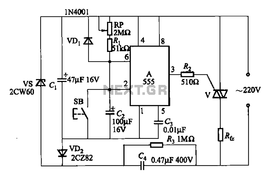
The 555 timer IC is a versatile component widely utilized in various timing applications, including delay circuits. In this configuration, the circuit operates in monostable mode, where it generates a single output pulse in response to a trigger input. The circuit consists of several key components: the 555 timer IC, a resistor, a capacitor, and a potentiometer for adjustable timing.
Upon pressing the switch SB, a low-to-high transition is detected, triggering the 555 timer. The capacitor connected to the timing circuit begins to charge through the resistor and the potentiometer RP. The time delay before the output transitions from high to low is determined by the values of the resistor and the capacitor, as described by the formula:
\[ T = 1.1 \times R \times C \]
Where T is the time delay in seconds, R is the resistance in ohms, and C is the capacitance in farads. By adjusting the potentiometer RP, the resistance can be varied, allowing for precise control over the timing interval.
Once the capacitor reaches approximately 63.2% of the supply voltage, the output of the 555 timer switches from high to low. The output remains low until the circuit is reset or the button SB is pressed again, which restarts the cycle. This functionality makes the 555 timer IC an excellent choice for applications requiring delayed actions, such as timers, pulse generators, and automatic switches in various electronic devices.
The circuit can be further enhanced by incorporating additional components, such as diodes for protection against reverse polarity or transistors for driving higher loads, depending on the specific application requirements.A 555 four-base integrated circuit delay circuits They are a jump from high to low transition of the delay circuit. That button is pressed SB snow, the output is high, after so me delay, the output of the transition to the low level and remain low. Adjustment potentiometer RP, can change the delay time.
Related Circuits
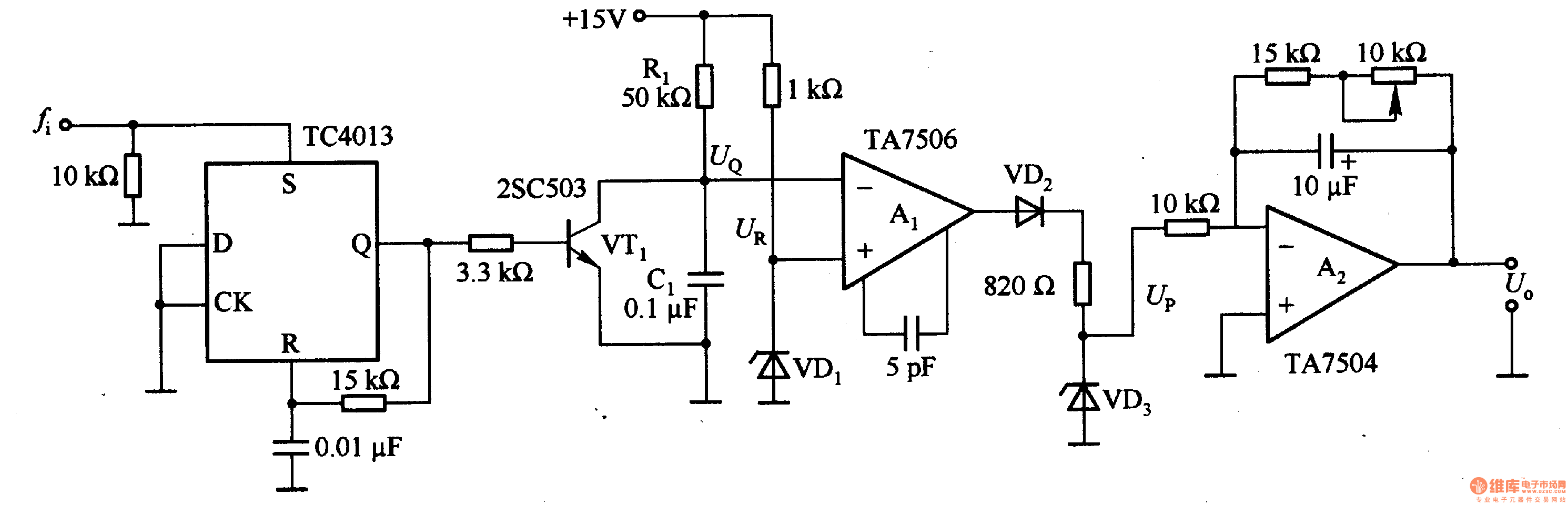
This circuit can convert an input frequency ranging from 0 to 100 Hz into an output voltage of 0 to 10 V. It utilizes the TC4013 monostable multivibrator to shape and amplify the input pulse, which has a width...
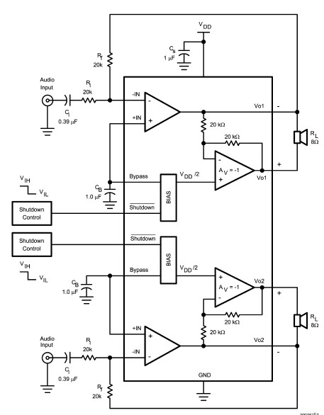
The LM4992 stereo audio power amplifier can be utilized to design a straightforward audio power amplifier project suitable for portable electronic devices. This amplifier circuit is capable of delivering 1 watt of continuous average power per channel to an...
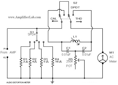
A circuit diagram of an audio distortion meter is presented here. An audio distortion meter is utilized to measure Total Harmonic Distortion (THD). The audio distortion meter is an essential tool in audio engineering, designed to quantify the level of...
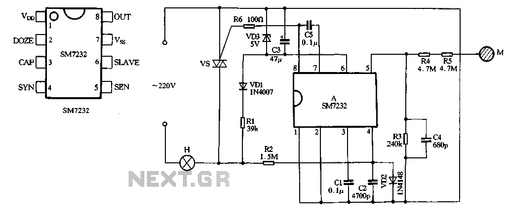
The core component of the circuit is the dimmer, utilizing the SM7232 integrated circuit. The pin configuration includes: 1) VDD, the positive power supply terminal; 2) DOZE; 3) CAP; 4) SYN, which synchronizes input power frequency using an internal...
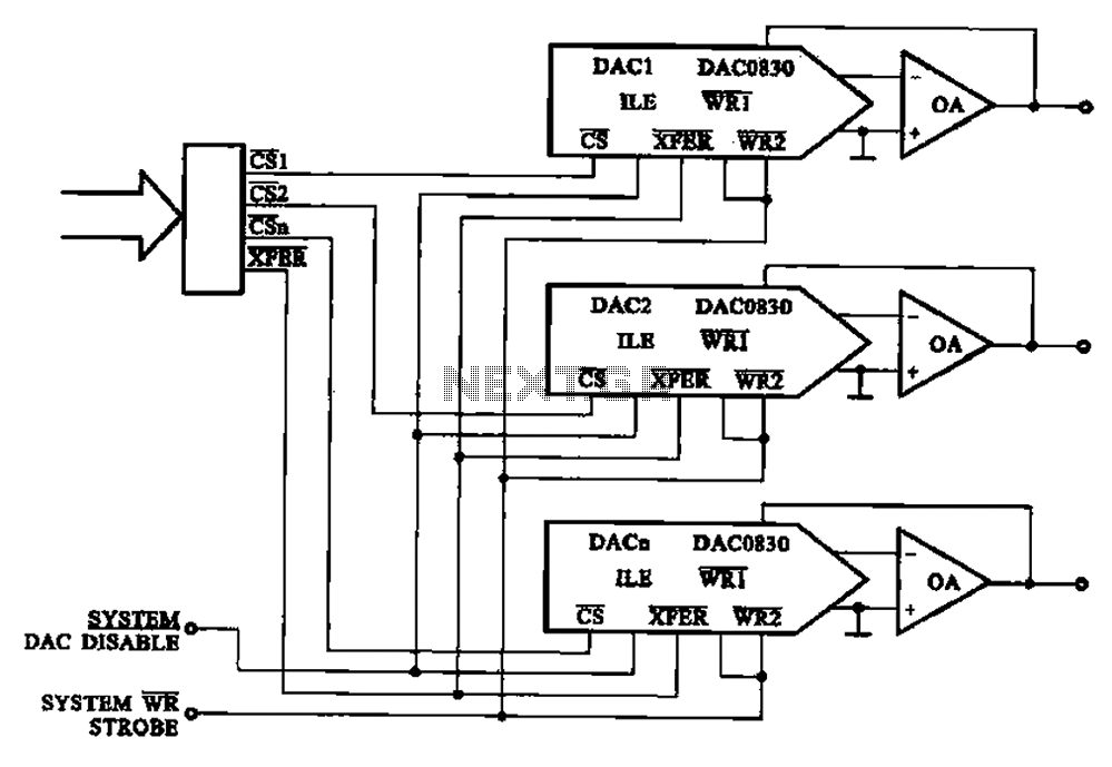
A multi-channel D/A converter circuit is presented, illustrating its fundamental structure. This circuit effectively converts encoded digital signals into multiplexed analog signal outputs. The multi-channel Digital-to-Analog (D/A) converter circuit is designed to facilitate the conversion of digital signals into corresponding...
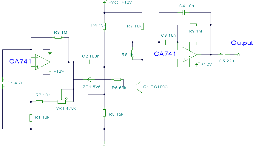
This circuit utilizes two operational amplifiers (op-amps) to create a unique sound effect. The first op-amp, CA741, is configured as a standard astable multivibrator, generating timing pulses controlled by components C1, R2, and variable resistor VR1. The output from...