
Accelerometer Signal Amplifier
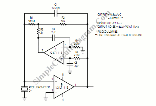
An inverting mode amplifier is a critical component in applications involving precision accelerometers, which often produce a charge output as a response to acceleration. The primary function of the inverting amplifier in this context is to convert the charge generated by the accelerometer into a corresponding voltage signal that can be easily processed and analyzed.
The inverting amplifier configuration typically consists of an operational amplifier (op-amp), a feedback resistor (Rf), and an input resistor (Rin). The input charge from the accelerometer is converted to a voltage by the relationship defined by the equation Vout = - (Rf/Rin) * Vin, where Vin represents the input voltage derived from the charge. The negative sign indicates that the output signal is inverted relative to the input signal.
To ensure precision in the conversion process, it is essential to select appropriate values for Rin and Rf. The gain of the amplifier can be adjusted by changing the ratio of these resistors, allowing for flexibility in application based on the specific characteristics of the accelerometer being used.
Furthermore, the design must account for factors such as bandwidth, noise performance, and stability, which are critical for maintaining the integrity of the signal in high-precision applications. The power supply for the op-amp should also be considered, ensuring that it meets the requirements for the desired output voltage range.
In summary, the inverting mode amplifier serves as an essential interface between precision accelerometers and the electronic systems that utilize their output, facilitating the conversion of charge to a usable voltage signal while maintaining accuracy and reliability in measurement.Inverting mode amplifier is needed by precision accelerometers because that usually charge output device. This amplifier is used to convert charge into voltage.. 🔗 External reference
Related Circuits
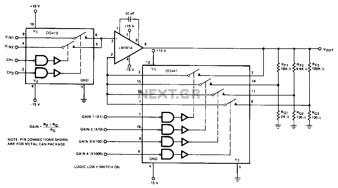
The DG419 considers the high input impedance of the operational amplifier, making the effects of Rvs negligible. The DG441 is also connected in series with RIN and is not included in the feedback dividers, thereby contributing negligible error to...
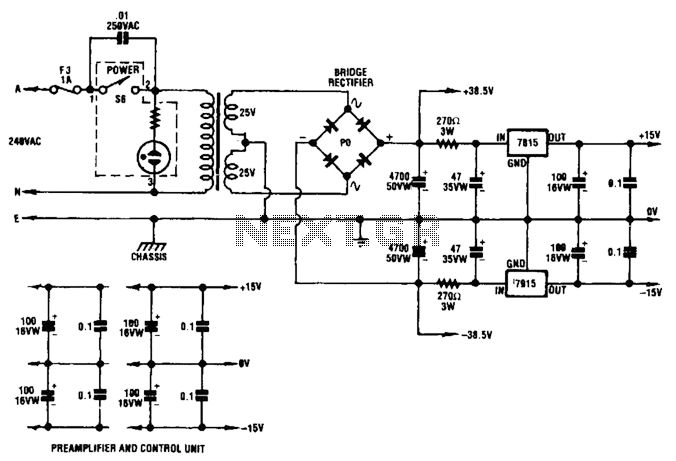
A dual audio amplifier that delivers 50 W per channel is illustrated in the schematic. It features a preamplifier and tone controls, as well as a headphone amplifier. The circuit also shows a power supply providing 38.5 V and...
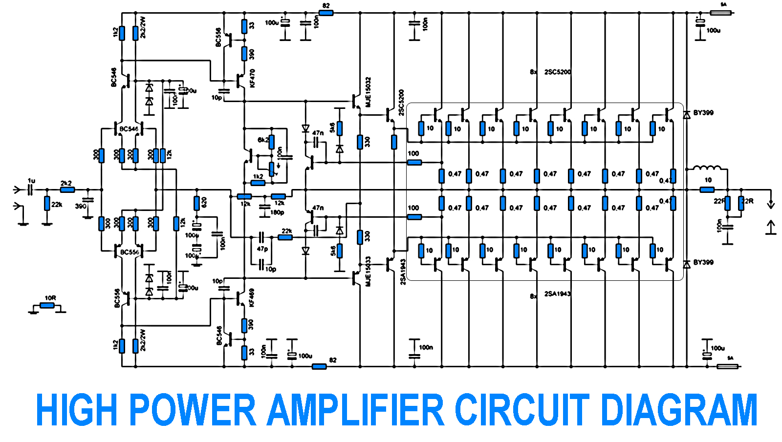
700W Amplifier. Adjusting the amplifier power to 700W appears straightforward, yet it is essential to consider the adjustment of the driving transistors and the frequency offset engagement. It is necessary to modify the current protection circuit that safeguards the...
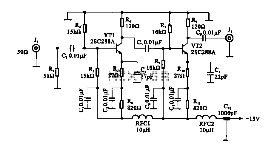
The circuit consists of a two-stage common emitter amplifier, which serves as a practical wideband amplifier. It utilizes capacitors for coupling between the input and output stages. The emitter decoupling capacitor, C4, is employed to eliminate AC negative feedback,...
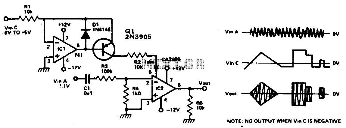
This circuit is essentially an operational amplifier (op-amp) with a differential input voltage of ±10 mV between pins 2 and 3, along with an additional input at pin 5. A current (Iabc) is injected to control the current at...
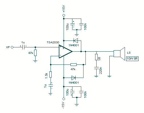
Although the TDA2030 can deliver 20 watts of output power, I deliberately reduced the output power to about 8 watts to supply 10 watt speakers. Input sensitivity is 200mV. Higher input levels naturally will give greater output, but no...
Warning: include(partials/cookie-banner.php): Failed to open stream: Permission denied in /var/www/html/nextgr/view-circuit.php on line 713
Warning: include(): Failed opening 'partials/cookie-banner.php' for inclusion (include_path='.:/usr/share/php') in /var/www/html/nextgr/view-circuit.php on line 713