
AD1865 based audio DAC with I2S input and voltage output
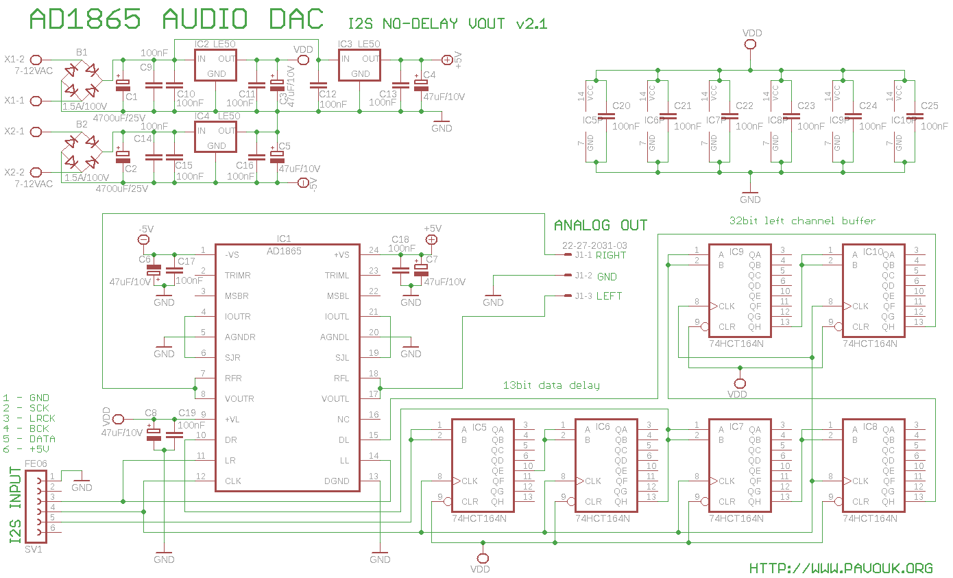
I used available low-drop voltage regulators LE50. One is for supplying of digital part and two are for positive and negative analog part of dac. Closely to regulators and integrated circuits are small filter and blocking capacitors. DAC doesn`t have I2S input, which is usual. It has individual data inputs for left and right channel and individual "latch" inputs which rewrites data from internal register to DAC output. Input data in I2S format (left justified) are first delayed for 13 bits thus that after shifting of 18 most significant bits to the dac register they will be written to output.
For simultaneous playing of left and right channel we must delay data of left channel for 32 clocks (frame lenght for one channel). Result is that data for left and right channel are shifted together to the dac and they are written to the output with common latch signal.
Because there doesn`t exists 32bit shift-register I had two choices. Create them with help of Xilinx, but I have not experience with it or assemble them from easily available 8bit shift-registers. I wanted to avoid variant with registers train. However prototype with CMOS 64bit register CD4517 doesn`t work thanks to different logic levels. On the end I had to use plenty of 74HCT164 which have 13 bits delay function and 32 bit register for left channel data.
Result exceeded my expectations and DAC is fully functional for signals up to 192kHz/24bit which is 12. 288MHz clock frequency. This time I choose voltage DAC output. Output has +/-3V at maximum deflection which must be enough for every amplifier. In rest is zero on the output. Respectively there can be small DC offset few milivolts. Output can be direct-current separated with high quality capacitor if offset matter. There are no one filter on the output limiting frequency. I count with filtering in next parts of audio chain like amplifier, speaker and ear. We assemble PCB from smaller parts to bigger. We begins with SMD capacitors and next with wire wraps. Circuits we can solder with small soldering iron and small 0. 5mm tube tin. In case of emergency we can use transformer soldering iron and bigger tin. When some of pads will be connected together, we can exhaust overflowing tin with solder wick. Next I installed IC5 to IC10 and small capacitors from top side and next voltage regulators, connectors, rectifiers, dac and last big capacitors.
PCB is designed single sided with four wire junctions. It help as to make them in amateur conditions. SMD parts are from a bottom side and parts with wires and connectors are from a top side. Supply wires are designed with accent on right ground wiring and junction of analog and digital ground in a one point. Block capacitors are very close to circuits. PCB has four assembling holes for mounting with screws. Design of this board was this time difficult thanks to big number of parts, but finally all components was on the pretty small board with only four wire connections.
After build of DAC I had to slightly modify board, because there was small digital noise visible on oscilloscope on one of the analog outputs. Now there are ground trac 🔗 External reference
Related Circuits
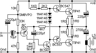
The circuit is very simple and incorporates darlington output transistors that will provide more than enough output current than is needed to drive a 3-ohm speaker. The gain may be pre-set for a variety of input levels, making it...

The oscillator is designed to tune from 1.8 GHz to 2 GHz for typical cellular telephony applications. An extended tuning range can be obtained by adjusting the ratio between the varactor capacitance and fixed capacitance in the tank. PMOSFETs...
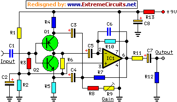
The objective of this project was to design a small, portable mixer powered by a 9V PP3 battery while maintaining high-quality performance. The mixer consists of three main modules that can be varied in number and/or arrangement to meet...
A typical circuit for applications such as mobile phones, MP3 players, and portable electronics utilizing the SSM2602 Low Power Audio Codec is provided in the SSM2602 Applications Circuit Schematic. The SSM2602 Low Power Audio Codec is designed for high-performance audio...
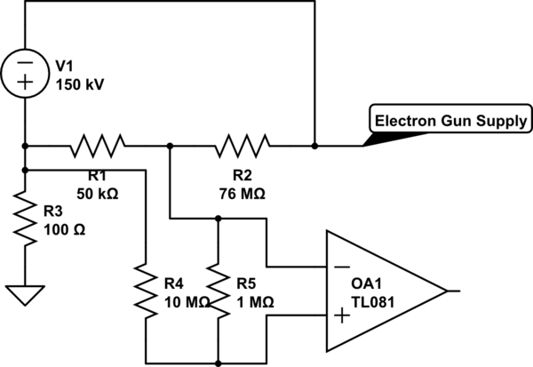
A high voltage power supply is designed for an electron beam system. The voltage regulator utilizes an outdated analog system that operates through a comparator and a reference signal from a potentiometer (POT). The challenge involves the feedback voltage...
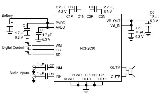
The NCP2830 audio power amplifier features high-quality audio performance with a total harmonic distortion plus noise (THD+N) of 0.04%. It offers low noise with a signal-to-noise ratio (SNR) of up to 100 dB and optimizes overall system efficiency, achieving...