
2 GHz CMOS Voltage-Controlled Oscillator with Optimal Design of Phase Noise and Power Dissipation

The oscillator circuit employs a cross-coupled LC topology, which is essential for generating the desired frequency range while maintaining stability and low phase noise. The choice of PMOSFETs contributes significantly to the overall performance, as their characteristics minimize 1/f noise, which is crucial for RF applications. The LC tank circuit, comprising the differential inductor and varactors, plays a pivotal role in determining the oscillation frequency and tuning capabilities. The differential inductor's design, with specific dimensions and a calculated Q factor, ensures efficient energy storage and transfer, while the varactors provide the necessary tuning range to accommodate frequency variations in cellular applications.
The use of a parallel LC filter tuned to twice the operating frequency enhances the circuit's ability to suppress unwanted noise, particularly from the biasing transistor. This design consideration is critical in achieving the low phase noise specifications required for high-performance RF applications. Furthermore, the careful selection of bias currents and transistor dimensions ensures that the differential pair operates within the saturation region, thus optimizing the oscillator's performance and minimizing phase noise contributions.
Overall, the oscillator circuit exemplifies advanced RF design principles, integrating various components and considerations to achieve a high-performance voltage-controlled oscillator suitable for modern cellular telephony applications. The resulting prototype demonstrates effective tuning, low phase noise, and efficient power management, making it a valuable addition to RF system designs.The oscillator is designed to tune from 1. 8 GHz to 2 GHz for typical cellular telephony applications. An extended tuning range can be obtained by adjusting the ratio between the varactor capacitance and fixed capacitance in the tank. PMOSFETs are employed in the design due to their low 1/f noise characteristics, critical for minimizing close-in ph
ase noise. The oscillator LC tank is composed of a single three-turn center-tapped differential inductor [17] with an inner radius of 150 m and trace width and spacing of 30 m and 3 m, respectively, and a capacitive network of MOS varactors and MIM capacitors. The inductor exhibits a differential inductance of 4. 6 nH with a Q of 15 at 2 GHz. P-channel MOS capacitors are used as varactors for tuning the oscillator frequency. The varactors are biased in the depletion region to achieve a capacitance range from 2. 4 pF to 1. 6 pF at VGB of -0. 4V and -1. 1V, respectively, while maintaining a high quality factor of over 30. To obtain the desired VCO frequency tuning range, additional high-Q MIM capacitors of 225 fF are included in the tank.
Another parallel LC tank consisting of Lfilter and Cfilter, tuned to twice of the operating frequency (2f0 = 3. 8 GHz), is employed to suppress the up-conversion mechanism of the baseband noise from the biasing transistor (M3), as proposed in [6], to minimize phase noise at low offset frequencies near the carrier.
Properly designing the differential pair transistors` mode of operation is crucial for achieving a low phase noise performance at minimal core bias current. Leeson`s phase noise equation [18] suggests that low phase noise performance can be achieved by enhancing the RF power or oscillation signal amplitude through increasing the oscillator core bias current.
However, designs aiming for a large oscillation swing with high current dissipation typically drive the differential pair transistors into a deep triode region, which severely degrades the oscillator loaded tank impedance and quality factor. High-Q tanks are especially prone to this type of operation. Fig. 2(a-c) presents an intuitive graphical illustration in describing the importance of ensuring the differential pair transistors to operate strictly in the saturation region.
Fig. 2(a) shows the RF signal power versus bias current on a logarithmic scale. Note that in the saturation region the signal power increases as a function of square of the bias current, I2 Once the bias current reaches to a level where the single-ended peak-to-peak oscillation amplitude exceeds the threshold voltage of the differential pair transistors, the active devices enter the triode region for a portion of the oscillation period. As the amplitude is further increased, the differential pair spends more of a period operating in triode, where the RF power does not increase as I2 due to the degraded tank impedance as depicted in Fig.
2(a). The thermal noise contribution of the biasing transistor, M3, typically dominates the VCO phase noise, which increases with its small-signal transconductance; hence, the square root of the bias current. Once the differential pair transistors enter the triode region, degraded tank impedance results in an output noise power profile with a reduced slope of less than I 1/2, as illustrated in Fig.
2(b). Combining Fig. 2(a) and Fig. 2(b) produces an oscillator phase noise profile as depicted in Fig. 2(c), indicating a dependence of I-3/2 in the saturation region. A further increase of bias current results in a negligible phase noise improvement in the triode region. Therefore, an optimal oscillator design trade-off between an achievable low phase noise and bias current can be obtained by ensuring the differential pair transistors do not operate in the triode region.
This thus calls for a single-ended peak-to-peak oscillation amplitude equal to the threshold voltage of the differential pair transistors for the chosen VCO topology. A prototype RF VCO is designed in the TSMC 0. 18 m 1. 8V non-epi process. Based on the components values described in Section II, the loaded LC tank impedance exhibits 230 © in the designed frequency range.
Therefore, a DC bias current of 2. 67mA is required for obtaining a single-ended peak-to-peak oscillation amplitude of 0. 8V (the value of the PMOS threshold voltage with body effect). W/L of 64 m / 0. 18 m for the differential pair transistors are thus needed to achieve a small-signal loop gain of 2 to ensure a proper oscillation startup. The biasing transistor is sized at 64 m / 0. 48 m. The non-minimal channel length is selected to minimize the device 1/f noise contribution. The W/L is designed to be as small as allowed to ensure its operation in saturation while minimizing its thermal noise contribution to the oscillator phase noise.
Lfilter of 4. 28 nH and Cfilter of 410 fF are employed to achieve a resonance of 3. 8 GHz for Fig. 3 presents the micrograph of the VCO chip occupying an area of 1 mm x 1 mm including pads. The LC tank inductor occupies an area of approximately 550 m x 550 m. The oscillator core is interfaced with an on-chip buffer, which exhibits an attenuation factor of 0. 25 and is properly matched to 50 © impedance for external characterization. The VCO is tunable from 1. 8 GHz to 2. 0 GHz with 0. 7V (0. 4V < Vtune < 1. 1V). Fig. 4 shows the oscillator output power spectrum at 2 GHz, displaying -10 dBm RF power with 2. 67mA bias current dissipation from a 1. 8V supply. The measured time domain waveform The oscillator achieves a phase noise of -103 dBc/Hz at a 100 kHz offset from the 2. 0 GHz carrier and reaches -125 dBc/Hz at 2 MHz offset frequency, limited by the noise floor of the measurement equipment.
Fig. 6 plots the measured phase noise at 100 kHz offset frequency as a function of the oscillator bias current for center frequencies of 1. 8 GHz, 1. 9 GHz, and 2. 0 GHz. The plot shows that a low phase noise is reached at the optimally designed bias current of 2. 67mA. At this current level, the differential pair transistors are operated strictly in the saturation region when they are on.
Further increase in bias current drives the transistors into triode without any significant phase noise improvement. The phase noise measured beyond 2. 67mA of bias current exhibits a variation less than 1 dB. The measurement also shows a 4-5 dB phase noise difference between the bias currents of 1. 67mA and 2. 67mA, thus following the phase noise The oscillator performance can also be characterized by using a figure of merit (FOM), which takes into account the phase noise, center frequency, offset frequency, and DC power dissipation [19].
The calculated VCO FOM with a center frequency of 2 GHz and offset frequency of 100 kHz versus bias current is shown in Fig. 7, indicating An RF VCO design optimization strategy to achieve low phase noise and low bias current is presented for a cross-coupled LC
🔗 External reference
Related Circuits
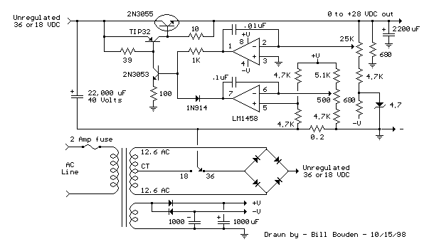
Since my page was first posted, I have received a number of emails asking about a high current power supply. I looked around, but couldn’t find one that was suitable. So, I designed this. It is a linear supply,...
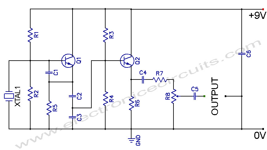
Crystal Controlled Oscillator Circuit. This general-purpose signal source is highly effective in signal-tracing applications. The output level is adjustable. The crystal-controlled oscillator circuit is designed to provide a stable and precise frequency output, which is essential for various electronic applications,...
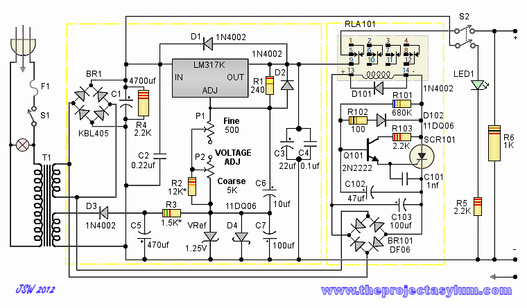
Another adjustment of application operational amplifiers to adapt a power supply is apparent below. The power supply requires an additional adjustment to supply the op-amps with a bipolar voltage (+/- 8 volts), and the negative voltage is also used...
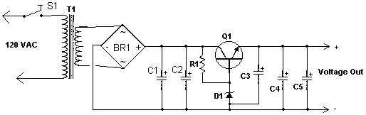
This power supply circuit operates using 120 volts from household mains and should only be undertaken by individuals with the appropriate knowledge and skills to safely construct such a project. Failure to do so may result in personal injury...
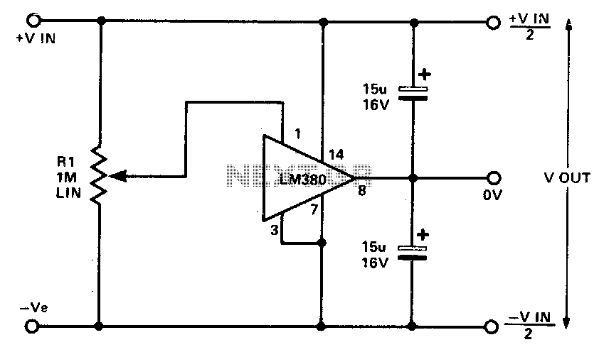
This circuit employs the quasi-complementary output stage of the well-known LM380 audio power integrated circuit (IC). The IC is internally biased to maintain the output at a midpoint between the supply rails when there is no input signal. A...
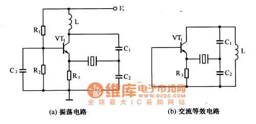
The oscillator that consists of a quartz crystal can be classified into two types: the parallel resonant type crystal oscillator and the series resonant type crystal oscillator. The parallel resonant type crystal oscillator and its AC equivalent circuit are...