
Atmel 89C2051 In-Circuit Programmer
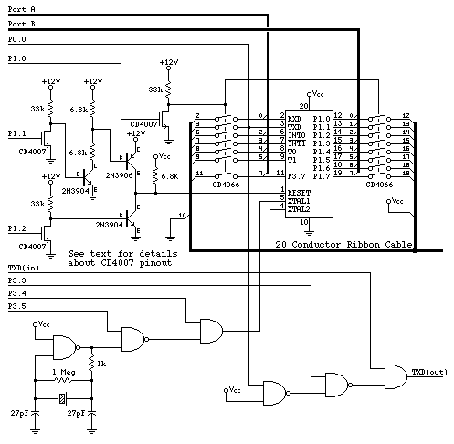
The described schematic integrates a beta release circuit designed for use with an 82C55 I/O chip and an 8051 microcontroller. This circuit is intended to enhance the existing system by providing additional I/O ports (A, B, and C) while requiring careful memory mapping to function correctly. The incorporation of 74HC08 and 74HC00 logic gates facilitates necessary signal processing, while the configuration of the CD4007 chip allows for the implementation of NMOS transistors that are crucial for the circuit's operation.
The schematic indicates specific connections that must be adhered to, particularly concerning the TXD signals, which are essential for serial communication and debugging. The echo-through feature is a significant aspect of this design, enabling real-time feedback during code execution, which can be invaluable for developers working with the 89C2051 microcontroller.
The requirement for specific voltage levels, particularly the +12 volts to pin 14 of the CD4007, emphasizes the need for careful power management to prevent damage to the components. The detailed explanation of the memory addressing scheme highlights the complexity of programming the 89C2051, necessitating either hardware modifications or software adjustments to ensure compatibility with the beta version.
Overall, the schematic presents a sophisticated solution for enhancing microcontroller functionality, but it also comes with caveats that must be considered by users. The next beta release is anticipated to resolve some of these issues, paving the way for a more user-friendly experience.This is a "beta release" schematic. Use at your own risk The idea is to add this circuitry to a board with already has ram at 2000 and an 82C55 I/O chip to provide ports A, B and C. Warning: not shown here is a memory mapping trick which is described below. You must figure out a way to provide the necessary memory mapping to make beta version 0. 00 3 work. The next beta release will fix this problem, so that an ordinary memory configuration will work. but for now a hardware trick or some preprocessing of your intel hex files is needed. The AND and NAND gates shown should be 74HC08 and 74HC00 respectively. It a TTL type NAND gate is used (eg LS, L, S, ALS, etc) the crystal oscillator may be problematic. NOTE: in the above schematic, the line indicated P3. 3 (which controls the TXD echo feature) should really connect to P3. 4, and the one labeled P3. 4 really ought to connect to P3. 3. Sorry. I`ll get a fixed copy of this schematic on-line sometime, with the signals names that now appear in BETA Version 0. 004. On the bright side, if you do connect it differently, it`s a simple matter to reassign the pins in the software with 0.
004. The inputs on the left side of the schematic come from the ports on the 8051 and 82C55. Port A, Port B, and PC. 0 come from the 82C55, and the other lines are from the 8051. The TXD pin of the 8051 is connected to the TXD(in) input line, and the TXD(out) line is connected to the line driver for the programmer`s serial transmit. This simple three gate circuit provides the "echo-through" feature which is useful for troubleshooting code while the 89C2051 is in-circuit by echoing data to the programmer`s transmit line.
The three NMOS transistors are within a single CD4007 chip. The trick here is to not use the three PMOS transistors which also come in this chip. You must connect +12 volts to pin 14. I`ll add more more detailed information about how to connect this chip, hopefully in a week or so. let me know if you`re building from this beta schematic and need some assistance. Basically, the two PMOS transistors with floating drains get their drains and sources connected to Vcc. The third PMOS transistor whose drain is connected to an NMOS drain inside the chip gets it`s source (the other line) connected to the drain, which is also the drain of one of the NMOS transistors.
Pin 14 MUST be connected to +12 volts to avoid damage to this chip. Warning: beta code 0. 003 expects RAM to exist at location 0x2000 to store a copy of the data to be programmed into the 89C2051. The code for the 89C2051 must be assembled at location 0000. Beta version 0. 003 uses the download code from the unreleased version of paulmon2, without any modification. When you download the code, beginning at location 0000, it really needs to get stored at location 2000, and so on.
To accomplish this, I just AND`d the Y0 and Y1 lines from the 74HC138 chip. However, for the development board example, this prevents the EPROM from working. I used the built-in EPROM in an 87C51 for the first version of this project, so this isn`t a problem. If you have an 87C51 and a programmer for it, this is the easiest way to make it work. For now, beta version 0. 003 requires some sort of hardware trick so writes to 0000 go into 2000, and so on. An alternate workaround is to assemble at 0000 and then modify the intel hex code to shift everything to location 2000, so that the download code will just write the data where the programmer needs it to be.
Here is some C source code to read and write intel hex files, if you want to take this approach. This isn`t a problem with BETA version 0. 004 since 0. 004 does address translation in software. All you have to do is specify the physical location of the buffer memory near the top of the program (in an. equ line), reassemble (as31 works), and 0. 004 will use this buffer memory when the user tries to download/upload/view code assembled starting at 000
🔗 External reference
Related Circuits
This document describes the HSETI PCB. This PCB is a small simple application for the Atmel AT89C2051 microprocessor - a 20 pin 8051 variant, with FLASH (reprogrammable) program memory. The board has just two chips on it, the CPU...

This circuit is simple to build and utilizes ICProg or Vellemann's K8076 picprog 2009 as the programming software. A serial device driver is required for NT4, Windows 2000, or Windows XP, while compatibility with Vista or Windows 7 is...

The Flash MC Programmer II is a rapid parallel port programmer designed for various 40-pin 8051 microcontrollers. The Flash MC Programmer II employs a parallel port interface to facilitate high-speed programming of 40-pin 8051 microcontrollers. This device is particularly advantageous...
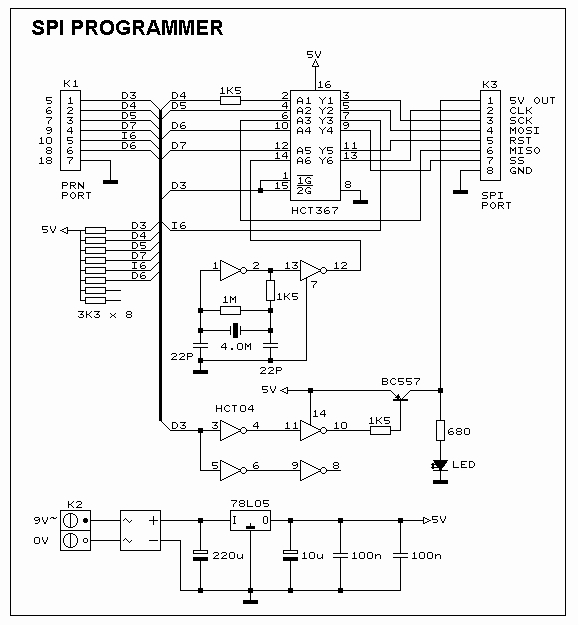
The image below displays the schematic diagram of the SPI Flash programmer hardware interface. Power for the interface can be supplied using either a 9V DC adapter or a 9V battery. The 74HCT367 integrated circuit (IC) buffers the adjacent...

This circuit allows for the easy programming of AVR microcontrollers including the AT90S1200, AT90S2313 (or ATtiny2313), AT90S8515, and AT90S4414, utilizing the free programming software PonyProg by Claudio Lanconelli. The software can be downloaded for free from the author's website....
This ISP Programmer can be utilized for in-system programming or as a standalone SPI programmer for Atmel ISP programmable devices. The programming interface is compatible with STK200 ISP programmer hardware, allowing users of STK200 to also use the software...
Warning: include(partials/cookie-banner.php): Failed to open stream: Permission denied in /var/www/html/nextgr/view-circuit.php on line 713
Warning: include(): Failed opening 'partials/cookie-banner.php' for inclusion (include_path='.:/usr/share/php') in /var/www/html/nextgr/view-circuit.php on line 713