
Audio AGC amplifier circuit

The Audio AGC circuit is designed to enhance audio signal processing by automatically adjusting the gain of the amplifier based on the input signal level. This is crucial in applications where audio signals can vary significantly, ensuring consistent output levels without distortion. The circuit's dynamic range of over 50 dB allows it to accommodate a wide range of audio input levels, making it suitable for various audio applications, including broadcasting and recording.
The use of P-channel JFETs (VT2 and VT4) is significant due to their high input impedance and low noise characteristics, which are essential for maintaining audio fidelity. The resistor divider network (R2, R3, R4, R10, R11, R12) plays a vital role in setting the input sensitivity of the AGC circuit. By distributing the input signal evenly, it ensures that the AGC reacts appropriately to changes in input levels.
The circuit's functionality is based on the principle of feedback. When the input signal is below the threshold of 40 mV peak-to-peak, the AGC circuit remains inactive, allowing the audio signal to pass through without alteration. However, as the input signal increases beyond this threshold, the AGC circuit engages, effectively controlling the gain to prevent distortion. This is achieved by manipulating the gate voltage of the JFET, which adjusts the channel resistance and allows for precise control over the output signal level.
Overall, the Audio AGC circuit is a sophisticated solution for managing audio signals, providing both stability and quality in audio applications. Its design ensures that the output signal remains within optimal levels, thereby enhancing the overall listening experience. Audio AGC can keep track, monitor audio preamplifier output signal level when the input signal increases, AGC circuit automatically reduces the gain of the amplifier; when the input signal is reduced, AGC circuit automatically increases the gain of the amplifier, so that an a/D signal is maintained at an optimum level, but also make the clipping is minimized. As shown in FIG audio amplifying circuit AGC, dynamic range greater than this amplifier 50dB, the output waveform distortion is very small, and has started fast, slow decay advantages.
Circuit input 40 ~ 20mV and 0 ~ 1.2V adjustable output level, a single power supply, current consumption less than 1mA (5V voltage). VT2, VT4 P-channel JEFT, it R2, R3, R4 (R10, R11, R12) constituting the equivalent resistor divider input circuit access.
When the input level is lower than 40mV (peak to peak), the input evenly between R2 and R3, R4 distribution, A1 output amplitude is not large enough to make a positive peak detector VT2 conduction. The gate of the JFET pulled + 5V, pinch off the channel and it produces a very very high resistance from drain to source.
When the input voltage peak to peak higher than 40mV, VTl turned A1 in positive peak output, lowers the junction-type FET gate-to-source voltage. Channel resistance and to reduce the attenuation of the input signal, in order to keep Al peak to peak output voltage of about 1.2V.
Related Circuits
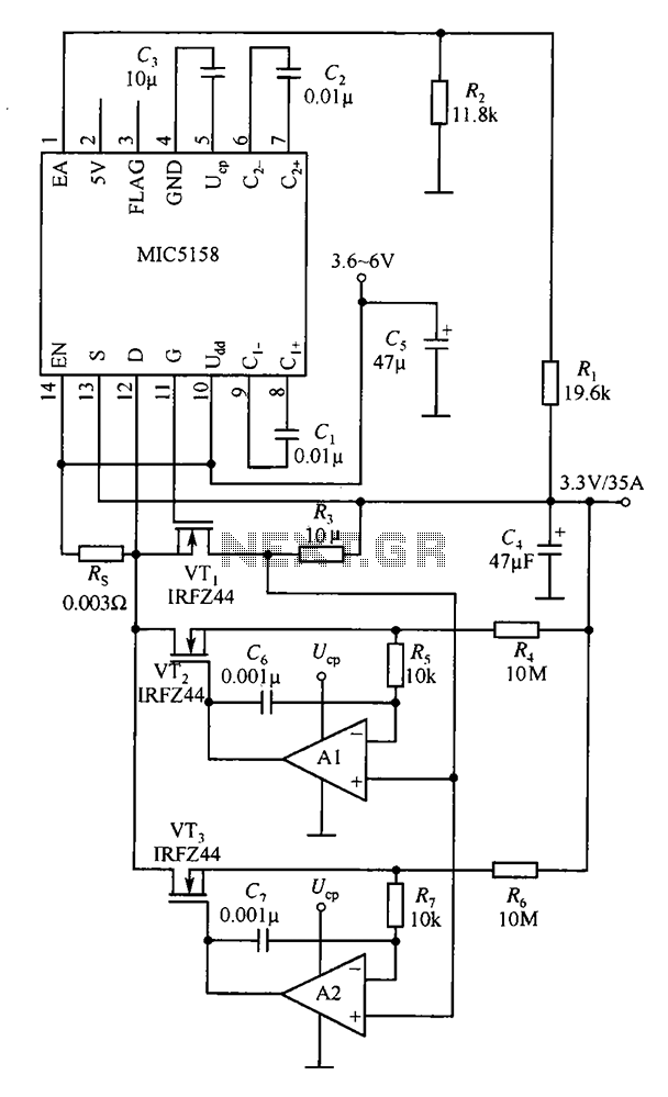
The MIC5158 is designed to manage tasks by controlling multiple external N-channel MOSFETs in parallel, which enables high current or high power output for a linear regulator circuit. This is illustrated in the accompanying figure. The operational amplifier circuit...
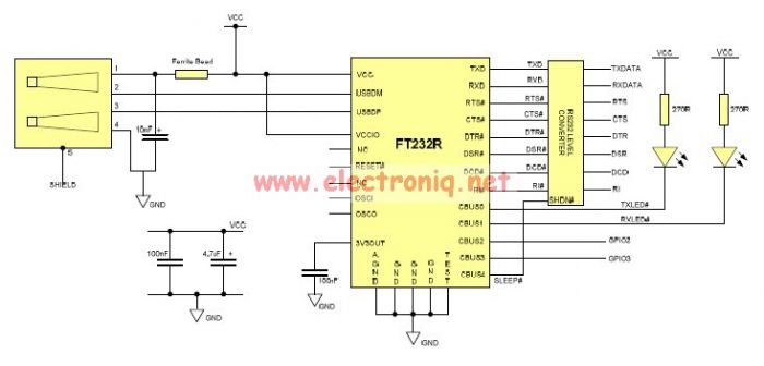
This USB to Serial RS232 adapter is highly beneficial in scenarios where a device with RS232 needs to be connected to a computer lacking an RS232 port but equipped with a USB port. Utilizing the FT232BM chip produced by...

During the recent audio hackers meetup at Hacker Dojo, discussions were held with Laura and Kevin regarding the challenges faced in creating a small local network referred to as "JamLan." There was mention of the consideration to develop a...
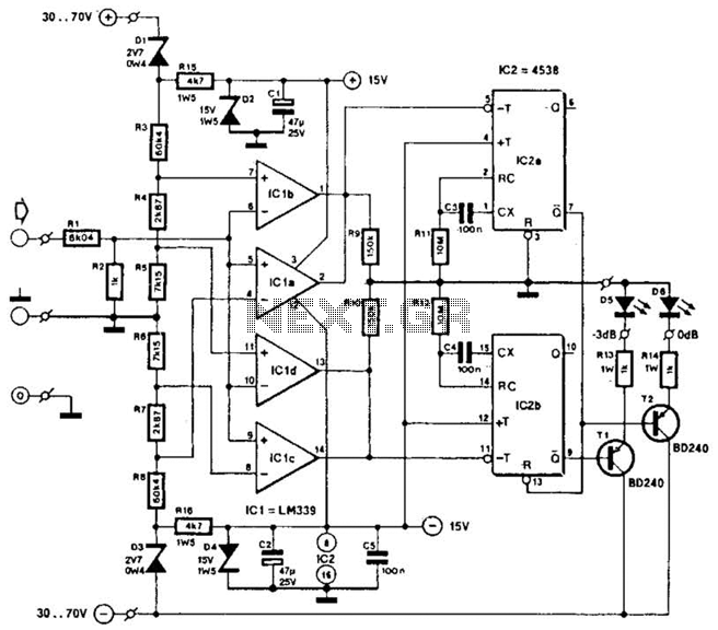
This circuit was utilized with an audio power amplifier to identify the point at which the output is -3 dB from maximum, indicated by LED D5, and at clipping, shown by LED D6. The indicator can be employed with...

An AC-coupled unity gain voltage follower operating on a single supply is illustrated. The voltage divider network consisting of resistors R1 and R2 provides a DC voltage equal to half the supply voltage to the non-inverting input of the...
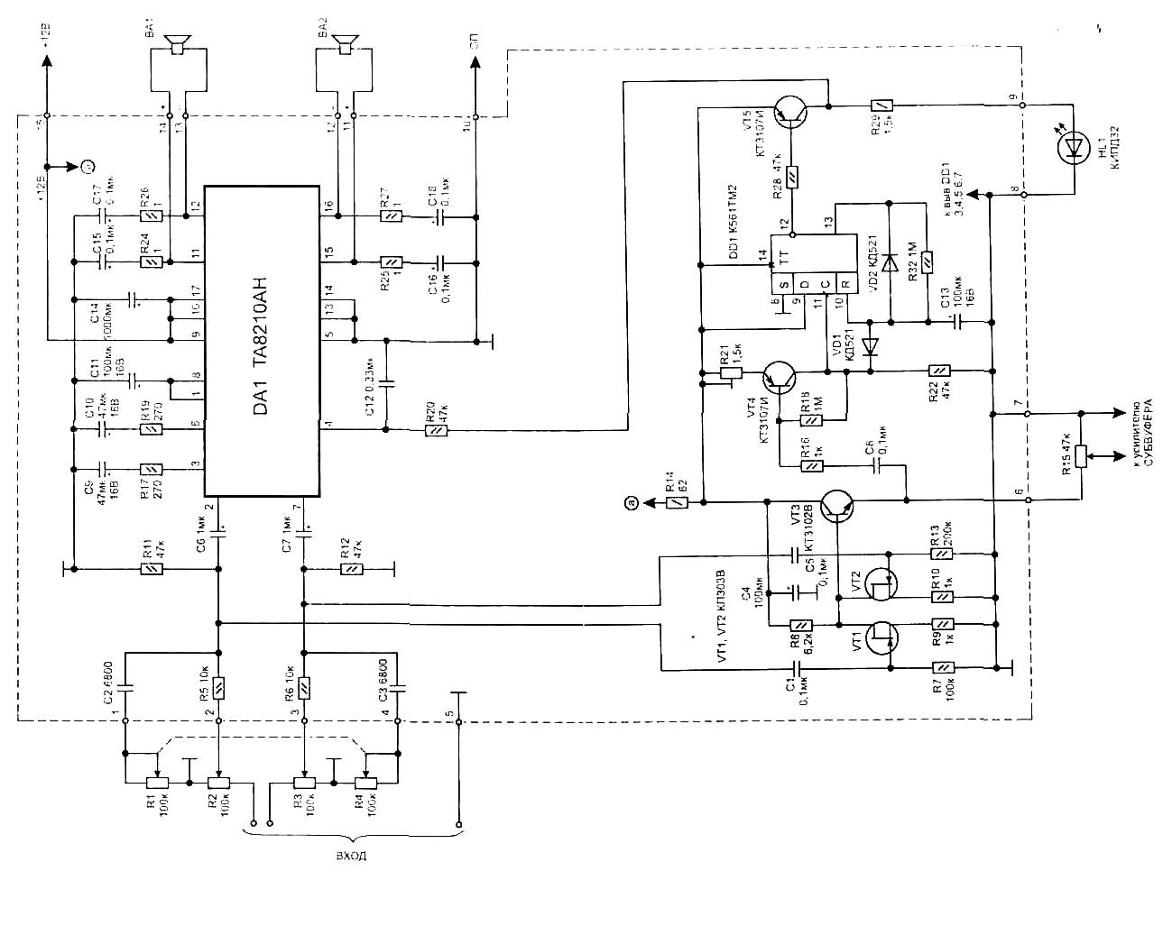
High-quality audio amplifier for computer circuit diagram. The electrical circuit of the amplifier is depicted in Fig. 1. The chosen integrated circuit for its construction is the TA8205AN, which is typically used in Hi-Fi applications due to its low...