
Voltage follower circuit

The described circuit functions as a unity gain voltage follower, which is an essential configuration in analog electronics. The primary role of this circuit is to buffer signals, providing high input impedance while maintaining low output impedance. This characteristic is particularly useful when interfacing high-impedance sources with low-impedance loads, ensuring minimal signal loss and distortion.
The voltage divider formed by resistors R1 and R2 sets the reference level for the non-inverting input of the operational amplifier. By configuring R1 and R2 to equal values, the non-inverting input is held at half the supply voltage, which is critical for AC coupling as it allows the output to swing symmetrically around this midpoint. The operational amplifier (in this case, a 741) is configured with negative feedback, which stabilizes the gain at unity and minimizes distortion.
The coupling capacitors, C1 and C2, serve to block any DC component of the signal while allowing AC signals to pass through. This is crucial in applications where the DC offset must be eliminated to prevent saturation of subsequent stages. The choice of capacitor values can significantly influence the frequency response of the circuit; therefore, for low-frequency applications, larger electrolytic capacitors are advisable to ensure that the cutoff frequency remains well within the desired operational range.
The input impedance, calculated as 500K Ohms, indicates that the circuit will not load down the source, preserving signal integrity. The low output impedance, a result of the feedback mechanism, allows the circuit to drive subsequent stages effectively without significant voltage drop. This configuration is widely used in audio processing, sensor interfacing, and other applications where signal integrity is paramount.An AC coupled unity gain gain voltage follower operating on a single supply is shown here. The voltage divider network of R1 and R2 provides a DC voltage equal to half the supply voltage to the non-inverting input of the 741. The output DC voltage therefore stands at half the supply voltage. The output signal swings above and below this value. The sta nding DC voltage at pin 6 does not matter because the output is coupled to the next stage via a capacitor. The input impedance is equal to the value of R1 and R2 in parallel, i. e. 500K Ohms in this case. Because of hundred percent negative feedback, the output impedance is very low. For low frequency applications C1 and C2 can be replaced by electrolytic capacitors of large values. 🔗 External reference
Related Circuits
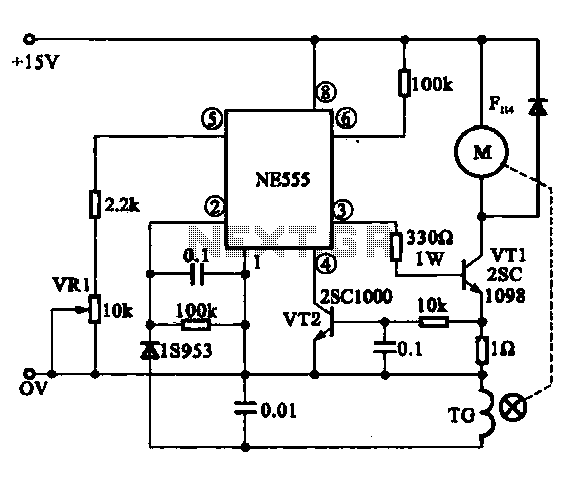
The Miniature DC Motor Speed Control circuit is designed to maintain a steady speed for micro motors, as illustrated in Figure 8-32. The circuit utilizes a voltage feedback mechanism suitable for applications such as tape recording machines that employ...
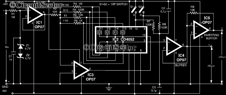
This circuit is a precision amplifier with digital control, designed for signal conditioning of low-output transducers operating in the millivolt range. The resistors R3 to R6 can be user-selected, with values ranging from 1 kilo-ohm to 1 mega-ohm, allowing...

This is a circuit design for an FSK demodulator, which is an electronic device that converts an FSK signal into a serial digital signal. FSK modulation is used to transmit digital serial data, and demodulation is necessary to retrieve...
This bat detector circuit was created by Chris Eve. Initial tests with various salvaged electret microphones demonstrated a good response to frequencies of 50 kHz and higher, with smaller units performing better. Tests indicate that a small electret microphone,...
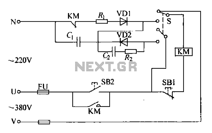
The AC contactor operates silently, demonstrating significant energy-saving effects, low noise, and a reduced operating temperature, which contributes to an extended lifespan. It is widely utilized in the production industry. When the SB2 button is pressed, the N-terminal receives...
Protect your equipment with this compact 12V time delay relay circuit. The SMPS-based power supply of modern electronic devices is susceptible to voltage spikes. This 12V time delay relay circuit is designed to safeguard sensitive electronic devices by providing a...