
Receiver If Amplifier
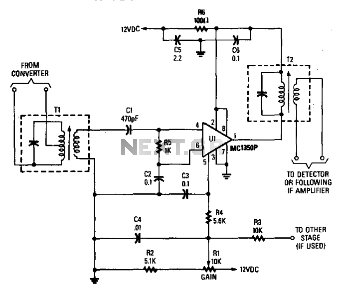
The circuit described involves a tuned amplifier configuration where Tl is optimized to match the output frequency of Ul, ensuring efficient signal amplification within the specified gain range of 45 to 50 dB. The gain variation is influenced by the characteristics and design parameters of the transformers Tl and T2.
The bypass capacitors C2, C3, C4, C5, and C6 are critical for maintaining stability and performance by filtering out unwanted AC noise and ensuring that the DC bias levels remain stable across the circuit. The inclusion of these capacitors helps to improve transient response and overall circuit reliability.
R5, as a bias resistor, plays a significant role in setting the operating point of the amplifier stages, ensuring that the transistors operate in the desired region for linear amplification. The gain control is achieved through Rl, which adjusts the voltage at pin 5 of Ul, allowing for fine-tuning of the amplifier's output level.
The impedance matching provided by Tl and T2 is essential for maximizing power transfer and minimizing reflections in the circuit. The specified source impedance of 1 kΩ and load impedance range of 3 to 10 kΩ are crucial for ensuring that the circuit operates efficiently within its intended application.
Additionally, R3 is included in the design to supply DC bias to other stages if necessary, further enhancing the versatility of the circuit by allowing integration with multiple amplifier stages or additional circuitry. This design consideration facilitates a broader range of applications while maintaining optimal performance characteristics. Tl is tuned to converter-output frequency Ul to provide 45-to-50-dB gain, depending on the design of Tl and T2. C2, C 3, C4, C5, and C6 are bypass capacitors. R5 is a bias resistor. Gain is set by Rl, which controls the voltage on pin 5 of Ul. Tl and T2 should provide source and load impedance of l-kft and 3- to 10-KOhmhm, respectively. R3 supplies dc bias to other stages, if required. 🔗 External reference
Related Circuits
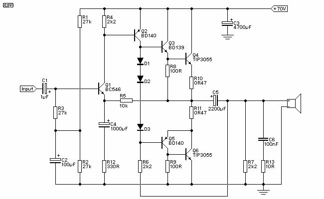
Figure 1 shows the circuit. A major change from all of the designs from that era is the speaker coupling capacitor - 1000uF (for a -3dB of 20Hz and a 8 Ohm load) was the most common value. This is...
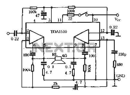
TDA1510 is an audio power amplifier from Philips. This integrated circuit (IC) includes features such as load short protection, open load detection, and an overheat protection circuit. It offers stable output voltage, excellent ripple rejection performance, requires fewer external...
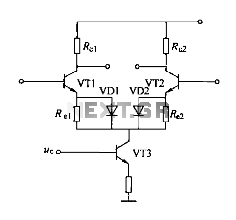
A controllable gain amplifier functions as an automatic gain control circuit within the execution unit. The primary methods for controlling the amplifier's gain involve two approaches: one is by adjusting certain parameters of the amplifier itself, such as emitter...
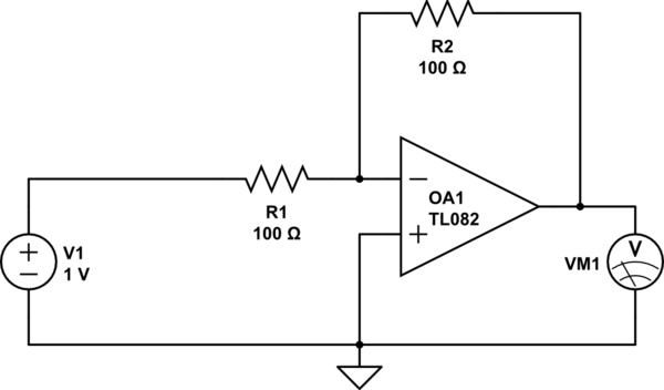
Considering a simple circuit as illustrated below, when the voltage source activates suddenly (changing from 0V to 1V), current will flow through the resistor R1. Assuming an ideal operational amplifier (op-amp) that draws no current, and an ideal voltmeter...
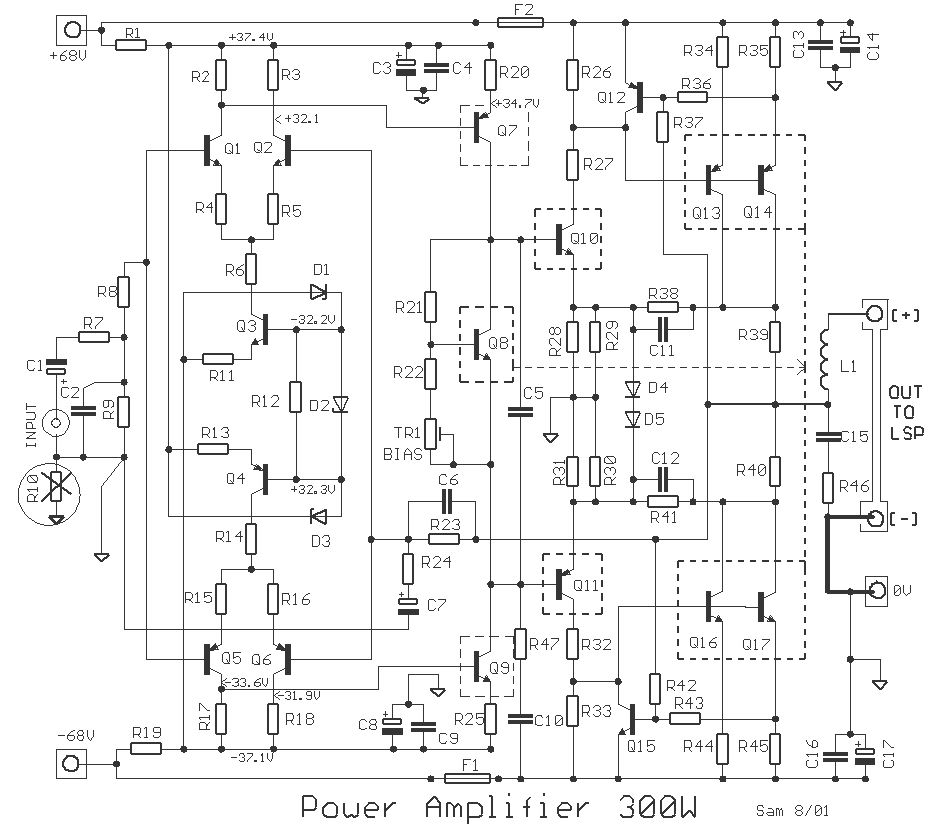
For many applications, there's no substitute for sheer power - low efficiency speakers, outdoor sound systems, or maybe you like the full flavor of the dynamic range of a high power amp. Whatever your requirement, this super power module...
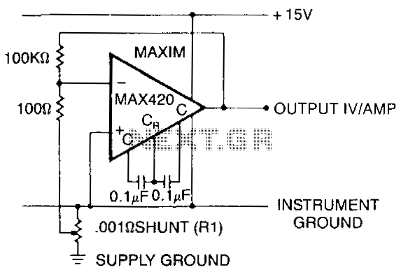
This circuit measures the power supply current of a circuit without using a current shunt resistor: R1 is only 3 cm of #20 gauge copper wire. A length of the power distribution wiring can be used for R1. The...