
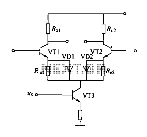
Emitter negative feedback differential amplifier gain control circuit
The controllable gain amplifier is designed to provide precise gain adjustments in response to varying input signal levels. The differential amplifier configuration utilizing transistors VT1 and VT2 allows for a balanced response to the input signals, ensuring that the output maintains fidelity. The use of emitter degeneration via resistors and diodes helps stabilize the gain and improve linearity by reducing the effects of variations in temperature and transistor parameters.
The reference components specified, such as the 3DG6 transistors and 2CP41 diodes, are chosen for their performance characteristics suitable for amplifier applications. The resistor values are critical in determining the amplifier's gain, with R1 and R2 providing the necessary feedback to maintain stability. The controllable attenuator implemented in the circuit allows for additional flexibility in gain adjustment, enabling the amplifier to adapt to fluctuating signal conditions effectively.
This design is particularly useful in applications requiring automatic gain control, such as audio processing, RF signal amplification, and instrumentation. By maintaining a consistent output level despite variations in input signal strength, the controllable gain amplifier enhances the overall performance and reliability of electronic systems. The careful selection of components and configuration ensures that the amplifier can handle a wide range of input conditions while minimizing distortion and maximizing signal integrity.Controllable gain amplifier is an automatic gain control circuit of the execution unit, the main method of controlling the gain of the amplifier in two ways: One way is through changing some parameters of the amplifier itself. As the emitter current, the load current distribution ratio, constant current source, and so to control the size of the negative feedback gain; Another method is to insert a controllable attenuator change the gain of the amplifier. Emitter negative feedback differential amplifier gain control circuit diagram shown. Component Parameters Reference values are as follows: 1) transistors 3DG6 2. 2CP41 diode. 2) Resistance: R. l a R spit a 5.lkfl, R. 1 a ReZ a Ra lkfl. VT1 and VT2 composed of the differential amplifier, the signal from VT1, VT2 base of two double-ended input, a collector from two double-ended output control signal.
Note from VT3 base into the two diodes VD1, VD2 and resistor R., ruler. composing emitter degeneration, and there R.l -Rcz -Rr, Rcl Rtz R. diodes VD1, VD2 conduction or not depends on Rel and R sweet drop. when the control voltage u. is small, IcJ small, and the average current flowing through the R. Re2 on each of Ie3/2. as kRt/2 is smaller than the diode turn-on voltage of the diode VD1, VD2 cut stop, then the minimum gain of the differential amplifier when the control voltage it increases, I increase, so Iea Re/2 is greater than the diode conduction voltage is VD1, VD2 conduction, conduction resistance rd will conduct current ID as Yun increases. visible, use when this gain control circuit, the control voltage H. should decreases as the input signal.
Related Circuits
At the input of the operational amplifier, a resistor-diode network can be constructed to create a square-law function conversion circuit. This resistor-diode network acts as a voltage divider, where the input voltage variations lead to different partial pressures. The...
The motor is rated at 6W, which corresponds to a current of 0.5 amps at a voltage of 12V. It is recommended to use a 12V DC power supply with a rating of 1A or higher. Any type of...
A power inverter converts direct current (DC) power to standard alternating current (AC) power. The following schematic illustrates a 12V power inverter circuit diagram. The 12V power inverter circuit typically consists of several key components that work together to achieve...
For the past few days, research has been conducted on an intriguing boost circuit known as the Joule Thief. The original schematic can be found through online resources. The Joule Thief is a simple yet effective boost converter circuit designed...
This is a compact LED flasher circuit designed using the 555 timer integrated circuit (IC), powered by two 1.5V batteries. The circuit can function as a flashing metronome, dark room timer, reminder, or for other similar applications. In the...
This infrared detector is capable of detecting the presence of modulated infrared signals in its vicinity from various electronic sources, such as an IR handheld remote. The infrared detector operates by utilizing a photodetector that is sensitive to infrared light....