
Bridge voltage regulator circuit diagram using the

The circuit configurations in Figures A, B, and C are designed to optimize voltage regulation under varying conditions. In Figure A, the bridge circuit is configured to ensure that the ratios of the resistors maintain a balance that allows for a high voltage coefficient, which is critical for applications requiring precise voltage levels. The output resistance, being a function of \( r_z \) and \( R_3 \), indicates that careful selection of these components can enhance performance by reducing losses.
In Figure B, the focus shifts to low voltage stability. The output voltage being the difference between two regulated voltages highlights the importance of selecting zener diodes with closely matched characteristics. This configuration is advantageous in scenarios where a consistent low voltage is required, such as in sensor applications or low-power electronic devices.
Figure C presents a more constrained application, where the voltage differential between the input and output is minimal. This setup necessitates precise matching of the zener voltages to ensure functionality. The equality of resistors \( R_2 \) and \( R_3 \) further stabilizes the output, making this configuration suitable for low-dropout applications.
Overall, these circuit designs exemplify various strategies for voltage regulation, emphasizing the importance of component selection and configuration in achieving desired electrical characteristics. Proper implementation of these principles can lead to improved performance in a wide range of electronic applications.FIG. A ~ c circuit has a high coefficient of voltage. If the regulator resistance rz is constant, while maintaining the delicate balance of the bridge situation has infinite vo ltage coefficient. Figure a load circuit connected to the bridge diagonal at the midpoint of regulation satisfies the condition R1/rz R2/R3, the output resistance of the circuit is about rz + R3. In order to reduce the voltage drop on R3, the output voltage should be stable with pressure pipe is equal to the operating voltage Uz.
Figure b circuit is particularly suitable for low voltage stable. The output voltage is approximately equal to the difference between the two operating voltage regulator, namely Uz1-Uz2. Output resistance is rz1-rz2 + R3. Figure c circuit is only suitable for input voltage and output voltage difference between a small case.
Two zener voltage should be as equal as possible the work, two resistors R2, R3 can be equal.
Related Circuits
Testing whether a transistor is shorted or open is typically performed using an ohmmeter. The test involves checking if current can flow between the base and emitter or the collector. To effectively test a bipolar junction transistor (BJT) for shorted...
Figure 4-11 illustrates a feedback attenuator that comprises a transistor-based tone control circuit. This circuit features a conventional high and bass control system, along with balance control, volume control, loudness adjustment, and subwoofer control, as well as field sense...
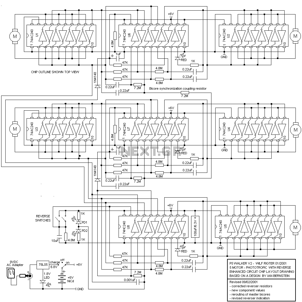
The P5 design utilizes eight 74HC/AC240 chips, which function as octal inverting buffers. Each 74HC/AC240 chip contains two groups of four inverters, each managed by a tri-state enable pin (pins 1 and 19). The 74AC240 chips (U1-U5) serve as...
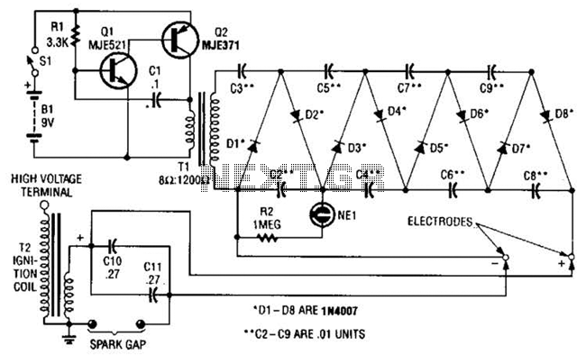
This circuit employs a transistor oscillator and a voltage multiplier to charge capacitors CIO and CI1 to a high voltage. When the spark gap breaks down, T2 generates a high-voltage pulse through the discharge of capacitors CIO and CI1...
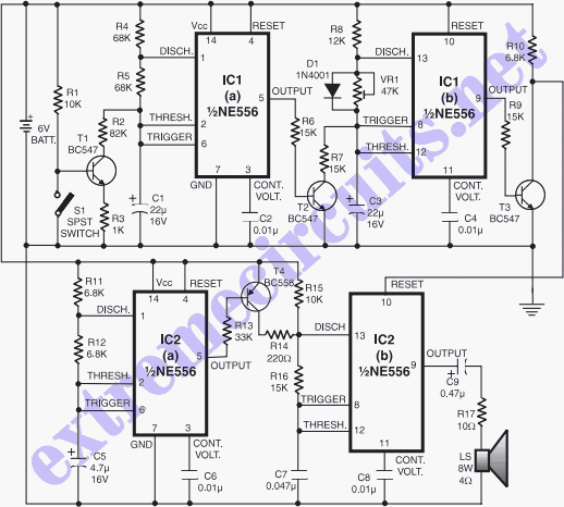
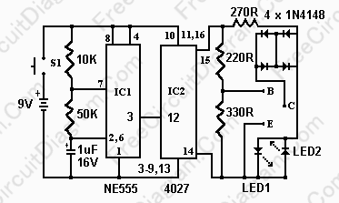
The circuit presented utilizes modulated rectangular waves of varying time periods to generate ringing tones akin to those produced by a telephone. It requires four astable multivibrators for operation, implemented using two 556 integrated circuits (ICs). The 556 IC...
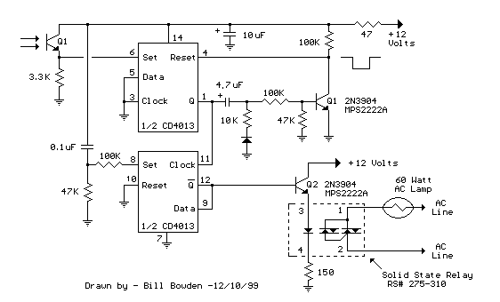
The IR photo transistor Q1 (Radio Shack 276-145A) or a similar component is connected to the set input (pin 6). It is essential to shield the photo transistor from direct light to ensure that the voltage at the set...