
Circuit explanation for the ultrasonic alarm
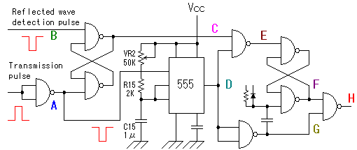
The alarm detector circuit utilizes a 555 timer configured in monostable mode to manage timing intervals effectively. The setup time is crucial, as it determines the window during which the presence of a reflected wave is monitored. The circuit's logic is designed such that any detected wave within this window resets the alarm condition, while the absence of a wave triggers the alarm output.
The SR-FF plays a significant role in maintaining the state of the alarm system. It is essential that the reset of the SR-FF occurs precisely at the rising edge of the 555 timer's output to ensure accurate operation. The differentiation circuit produces a pulse that controls the timing of the reset, ensuring that the system responds promptly to changes in the detection status.
Input protection is critical, particularly for N2, where D6 serves to limit voltage spikes that could damage the circuit. The design also incorporates careful consideration of voltage levels, especially during the timer's timeout phase, to prevent excessive voltage from affecting N2's input.
The overall architecture of the alarm detector circuit is tailored to provide reliable operation, with built-in safeguards to prevent false alarms and ensure the system only activates under the correct conditions. The integration of the 555 timer and SR-FF within the circuit allows for flexible timing control and state management, making it suitable for various applications in alarm detection systems.The alarm detector circuit is different from Ultrasonic Alarm (1). In Ultrasonic Alarm (1), an alarm output is presented when there is a reflected wave from the object in the setup time. At the circuit this time, an alarm is output when no reflected wave from the object is detected in the setup time oppositely.
The existence of the reflected wave in the setup time is detected like Ultrasonic Alarm (1) to do this operation. As for the time setting for 555 timer and so on, please refer to Alarm detector of Ultrasonic Alarm (1). The initialization of the circuit is done with transmission timing pulse (A). C to "L", D and F to "H", G to "L" by which D goes to "H". When a reflected wave is detected within the setup time of 555 timer, C goes to "H". With this, the E shifts to "L". When the E goes "L", F shifts "L" and it is held until the next initialization. G shifts to "H" when D goes "L" with the time-out of 555 timer. However, because F is "L", the alarm output H is held on "H" and an alarm signal isn`t output. The initialization of the circuit is done with transmission timing pulse (A). C to "L", D and F to "H", G to "L" by which D goes to "H". When a reflected wave isn`t detected within the setup time of 555 timer, the change of the E doesn`t occur.
It is held on "H". When D goes to "L" by the time-out of 555 timer, G shifts to "H". Because F is held on "H", H shifts to "L" and an alarm signal is output. Even if a reflected wave is detected behind the time-out of 555 timer, because D is held on "L" already, the change of the condition of E doesn`t occur. It is held on "H". So, the alarm output is kept. Alarm detecting circuit is composed of SR-FF (The set and reset type flip-flop circuit) and 555 timer.
The reset of SR-FF for alarm detecting which is composed of IC8 must be reset in the timing of the rising edge of the timer. The set and the reset of SR-FF are done by the L level. Therefore, the signal which reversed the output of the timer is used for the reset signal. Also, SR-FF must be reset only when timer operation is started. So, the pulse signal which is made with CR-type differentiation circuit is used. D6 is put for the input protection of N2. When the timer does in the time-out, the output of N1 shifts to the H level from the L level. At this time, an electric charge with power supply voltage is already stored up in C25. When there is not D6, 2 times of voltage of the power are applied to the input of N2. The forward voltage of the diode is less than 1V. So, the voltage to apply input of N2 becomes the forward voltage of diode + power supply voltage. In the left figure, a transmission pulse is used for the initialization of SR-FF(FF2) for the alarm detection.
In case of this circuit, normally initialization operation isn`t done. The problem is the time that the output of the timer becomes ON. It takes time the output of the timer becomes ON even if it starts 555 timers by the transmission pulse. FF2 is immediately reset by the transmission pulse and signal (4) becomes H level because of the high-speed operation of the NAND circuit.
As a result, alarm signal (5) occurs in short time to have drawn by the red line. This signal is several microseconds. However, it is enough time to make do the operation of the alarm hold timer. ( Refer to the schematic ) Therefore, the alarm hold timer has always operated At the circuit this time, the initialization of FF2 is done by the falling edge signal (3) of 555 timer. So, it doesn`t let out an alarm signal by the initialization operation. 🔗 External reference
Related Circuits
One of the critical components is a PWM speed controller, allowing for fine speed adjustments instead of just an "on" mode that runs at full power. This is important for safety. A basic stamp microcontroller was purchased, which includes...
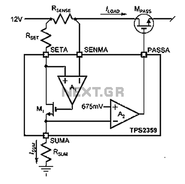
Amplifier A1 utilizes the voltage across the sense resistor sensors to monitor the load current ILOAD. The power management channel employs a similar circuit, with the distinction of integrating resistors RSENSE and RSET. Amplifier A1 is configured to measure the...
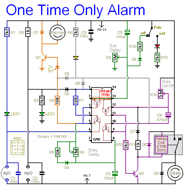
This alarm is designed to activate its siren only once. When the alarm is triggered, the siren will sound for a predetermined duration before turning off completely. The alarm will not reactivate automatically. The basic circuit features a single...
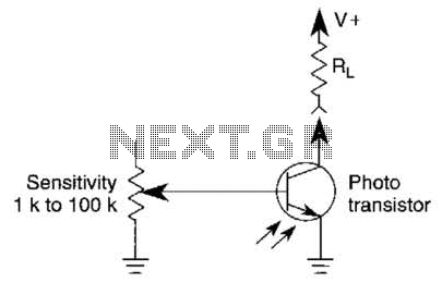
A variable resistor is utilized to adjust the light-level response of a phototransistor. Phototransistors exhibit higher light sensitivity compared to photodiodes; however, they typically demonstrate a lower frequency response. A variable resistor, often referred to as a potentiometer or rheostat,...
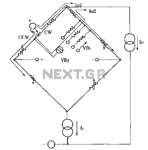
The circuit for zero and span adjustment consists of a feedback resistor network and a differential pressure sensing bridge measuring circuit. A constant current source, IO, represents the output current. The resistances of the four bridge arms are R1S,...
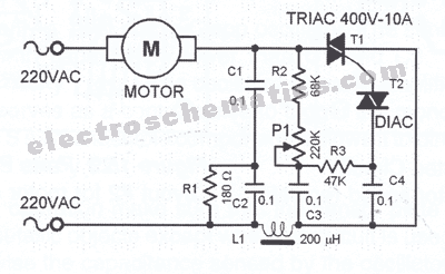
This triac-based 220V AC motor speed controller circuit is designed for controlling the speed of small household motors, such as drill machines. The motor speed can be adjusted by altering the setting of P1, which determines the phase of...
Warning: include(partials/cookie-banner.php): Failed to open stream: Permission denied in /var/www/html/nextgr/view-circuit.php on line 713
Warning: include(): Failed opening 'partials/cookie-banner.php' for inclusion (include_path='.:/usr/share/php') in /var/www/html/nextgr/view-circuit.php on line 713