
Circuit for ultrasonic threshold detection
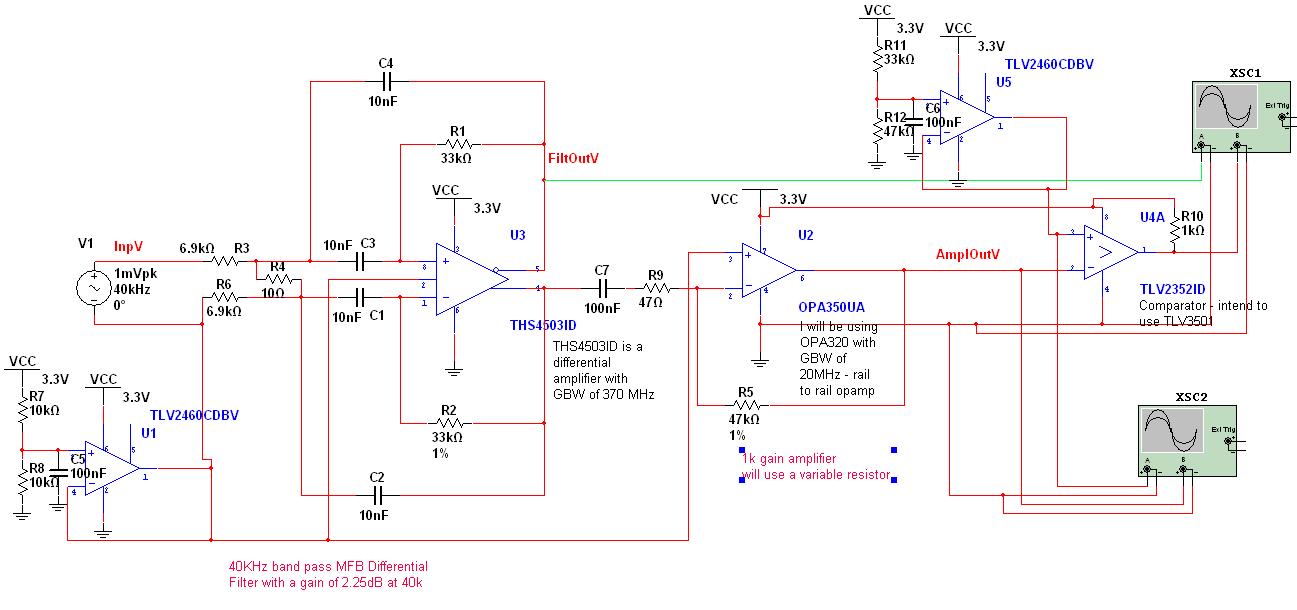
The circuit design focuses on accurately measuring the duration of ultrasonic pulses, which is crucial for applications such as distance measurement and object detection. The initial stage, consisting of a differential MFB filter, is essential for isolating the desired frequency from the ultrasonic receiver while ensuring minimal distortion. The choice of components, particularly the resistors in the feedback loop, influences the filter's performance. The deviation from the ideal resistor value may lead to slight shifts in gain and frequency response, warranting careful consideration during the design process.
For improved stability and performance, the implementation of bypass capacitors is vital. These capacitors should be strategically placed to ensure low impedance at the operational frequency, effectively filtering out high-frequency noise from the power supply. The selection of operational amplifiers is critical; while the OPA320 is a viable option, its limitations in bandwidth necessitate the exploration of alternatives such as the OPA2350. By distributing gain across multiple stages, the design can achieve the desired amplification without compromising stability.
The potential for oscillation due to capacitive loads must be addressed by selecting appropriate operational amplifiers and ensuring that the circuit remains stable across various load conditions. The TLE2426 offers a solution for generating a stable 1/2 Vcc reference, simplifying the design and enhancing reliability. The discrepancies in component values identified through simulation tools highlight the importance of thorough verification during the design process, ensuring that the final implementation meets the intended specifications.
In summary, the circuit's design should prioritize stability, gain distribution, and noise reduction while ensuring that the performance meets the requirements for ultrasonic pulse detection. Careful selection of components, along with rigorous testing and simulation, will contribute to the successful implementation of the circuit.I have designed the attached circuit for detecting how long an ultrasonic pulse need to to travel a distance. the input signal is going to be from a 40 k ultrasonic receiver. First stage is 40k Band pass - 1k pass band - differential MFB filter with a gain of 2. 25dB at Center frequency. In feedback path of differential amplifier I have used 33k in stead of ideal value of 31. 6k. I will appreciate some useful comments on how this circuit can be improved. Also I am going to design a PCB using smt components. I need suggestion to improve the circuit like adding capacitor to supply rail and VOCM which will reduce power supply noise etc. The TH4503doesprovidesthe necessary minimum gain-bandwidth (GBW) requiredto support your filter requirements.
The effect of using the 33k resistor willincreasethe gain slightly and move thecenter frequencydownby asmall amount. You can see the affects if you simulate the filter using TINA-TI. I can`t help but wonder why youchose touse the 33 k 1%, when 31. 6 k 1 % is a standard value too. I am concerned with attempting to get a gain of 1000 v/V at 40 kHz from a single stage. The OPA320 does not have sufficient bandwidth to supply that gain at 40 kHz. I suggestdividing the gain up equally between two operational amplifiers in a dual amplifier ( OPA2320 ).
The OPA320 appears to have about 55 dB of open-loop gain at 40 kHz and each stage would need 29. 5 dB of closed-loop gain -so there isn`t much loop gain left. The OPA2350 has about 5 dB more gain at 40 kHz so two stages may come closer in developing the 1000 V/V (60 dB) closed-loop gain you seek. A higher gain-bandwidth operational amplifier may be necessary. You willneed to place an effective bypasscapacitor path at each of the points where Vcc and the 1/2 Vcc voltage connects to the operational amplifiers.
These need to appear as a very low impedance at the frequency of interest. See the data-sheet for each amplifier you have selected for power supply bypass capacitor details. The TLV2460 operational amplifiers that drive the 1/2 Vcc lins may become unstable (oscillate) if the capacitive load on their output becomes too large. A device that is designed to provide the 1/2 Vcc function, eliminate the need for two matched resistors, and will drive a wide range of capacitance is the TLE2426.
There is a small possibility of oscillation under a certain load condition, but for your circuit doesn`t appear to be an issue (Fig 17 in data-sheet). I don`t know what filter synthesis program you used for the filter, but I do note a discrepancy in one component value when I check the circuit using TI`s FilterPro.
The input resistors (R1) are shown in your schematic as 6. 9 k. FilterPro produces a value of 12. 28 k. Possibly, one of my assumptions about your filter response is incorrect. The power supply bypass capacitors that you place on the 1/2 Vcc output levelappear as a capacitive load to the TLV2460 output. Addingabypass capacitancewith common valuesof 10 nF, 100 nF, or more, isconsidered alarge capacitive load.
The capacitive load, in conjunction with the amplifier`s output impedance, result in a pole that adds additional phase shift to the feedback loop. This reduces the phase margin and if at some frequencythe margingoes to zero degrees and the amplifier gain is great than 1 V/V, the circuit becomes an oscillator.
Different operational amplifier models willhave a different phase margin at the unity-gain cross frequency and their output impedance vs. frequency can be very different as well. Both are significant factors in determining whether a particular operational amplifier will be stable when driving a capacitive load.
You can usually find a graph inan operational amplifier`sdata-sheet indicating phase margin vs. load capacitance, or overshoot vs. load capacitance that will provide agood indication ofstability. 🔗 External reference
Related Circuits
This is a programmable clock timer circuit that utilizes individual LEDs to display hours and minutes. Twelve LEDs can be arranged in a circular pattern to represent the 12 hours on a clock face, while an additional 12 LEDs...
The circuit operates based on a desired temperature setting. It can be utilized for various applications, such as turning on a fan at a specified temperature or activating an emergency temperature alarm. The power supply for the circuit can...
The NJM2701 3D surround sound audio processor integrated circuit can be designed into a very simple 3D surround sound system. The NJM2701 reproduces 3D surround sound using only two speakers and is suitable for various audio applications, including micro-components,...
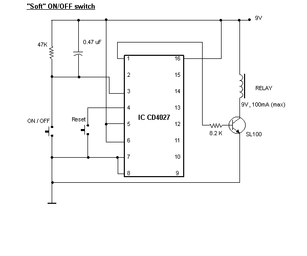
When the ON/OFF button is pressed once, the equipment goes on and stays on. It goes off when the button is pressed again. The circuit is straightforward. It uses a JK CMOS Flip-Flop with its JK terminals tied high...
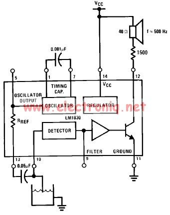
The LM1830 low-level detector can utilize an audio indication (speaker) or a visual indicator (LED - light-emitting diode) that activates when the level is too low. This low-level detector circuit generates a 500 Hz audio signal when the level...

When switches SW1, SW2, or SW3 are open, the input sensitivity is optimized for high-output devices such as CD players, tuners, tape recorders, iPods, miniDisc players, and computer audio outputs. The 750 Ohm value for resistors R3, R13, and...
Warning: include(partials/cookie-banner.php): Failed to open stream: Permission denied in /var/www/html/nextgr/view-circuit.php on line 713
Warning: include(): Failed opening 'partials/cookie-banner.php' for inclusion (include_path='.:/usr/share/php') in /var/www/html/nextgr/view-circuit.php on line 713