


Totem-Pole Output configuration found in ICs
#integrated circuits
#transistors
#output structure
#logic gates
#totem-pole
#IC design
#digital electronics
#high-low output
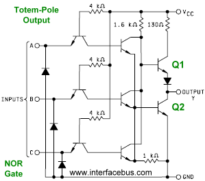
Description: A type of output structure used with integrated circuits in which one transistor drives the output high while another transistor connected below it pulls the output low. Many integrated circuits utilize Totem-Pole Outputs; in fact, it is so common that the output structure is not mentioned in the data sheet title. An integrated circuit with a Totem-Pole Output is the default condition, as opposed to an Open Collector Output, which is always indicated in the title of the data sheet. The circuit schematic below details the internal structure of a TTL triple input NOR gate with a Totem-Pole Output. The Totem-Pole is formed by transistors Q1 and Q2. The schematic and logic diagram are examples of 3-input NOR gates. The output structure will be some variation of a Totem-Pole, but the actual schematic will change depending on the Logic Family used. Note that the current paths differ between high and low pulses. A Totem-Pole output sources current to the load and sinks current from it. An output high is derived from Vcc through Q1, while an output low is derived from Q2 to ground. Therefore, a rising pulse encounters the impedance path of Q1, whereas a falling pulse encounters the impedance path of Q2. Depending on the logic function and the logic family, additional components may be present in one or both paths, in addition to the switching transistors Q1 and Q2. The different components and the varying impedances of the transistors result in a difference between the rise time and the fall time of the output pulse.
Totem-Pole Outputs are a fundamental design choice in digital logic circuits, particularly in TTL (Transistor-Transistor Logic) families. The architecture consists of two bipolar junction transistors (BJTs), where Q1 is responsible for pulling the output high and Q2 for pulling it low. This arrangement allows for a strong drive capability in both the high and low states, which is crucial for interfacing with other digital components.
In a typical application, when the input conditions dictate a high output, Q1 is activated, allowing current to flow from the positive supply voltage (Vcc) to the output. This creates a low impedance path to the load, ensuring that the output can drive multiple connected devices without significant voltage drop. Conversely, when the output is required to be low, Q2 is turned on, providing a direct path to ground and sinking current from the output. This dual action minimizes the time it takes for the output to transition between states, enhancing the overall speed of the circuit.
The rise and fall times of the output pulse are critical parameters in digital circuit design. The presence of additional components, such as resistors or capacitors, in conjunction with Q1 and Q2 can affect these timings. For instance, if a resistor is placed in series with Q1, it will slow down the rise time because it adds additional resistance to the current flow. Similarly, any capacitance at the output will introduce a time constant that affects how quickly the output can change state.
Different logic families, such as CMOS or ECL, may implement variations of the Totem-Pole configuration, leading to differences in output drive strength, power consumption, and speed. Understanding these variations is essential for selecting the appropriate logic family for specific applications, especially in high-speed digital circuits where performance metrics are critical.
In summary, the Totem-Pole Output configuration is a widely used output structure in integrated circuits, characterized by its ability to efficiently drive high and low outputs through a pair of transistors, Q1 and Q2. Its design considerations, including rise and fall times, are vital for ensuring reliable operation in digital applications.A type of output structure used with integrated circuits in which one transistor drives the output high while another transistor connected below it pulls the output low. Many ICs use Totem-Pole Outputs, in fact it`s so common that the output structure isn`t mentioned in the data sheet title.
An IC with a Totem-Pole Output is the default condition. As opposed to an Open Collector Output which is always indicated in the title of the data sheet. The circuit schematic shown below details the internal structure of a TTL triple input NOR gate with a Totem-Pole Output. The Totem-Pole is formed by transistors Q1 and Q2. The schematic and logic diagram are examples of 3-input NOR gates. The output structure will be some deviation of a Totem-Pole but the actual schematic will change depending upon the Logic Family used.
Note that the current paths are different between a high and low pulse. A totem-pole output sources current out to the load and sinks current in. Or an output high is derived from Vcc through Q1, and an output low is derived from Q2 to ground. So a rising pulse sees the impedance path of Q1 while a falling pulse see the impedance path of Q2. Depending on the logic function and the logic family there may be components in one or both paths in addition to the switching transistors Q1 and Q2. The different components and the different impedances of the transistors causes a difference between the rise time and the fall time of the output pulse.
Totem-Pole Outputs are a fundamental design choice in digital logic circuits, particularly in TTL (Transistor-Transistor Logic) families. The architecture consists of two bipolar junction transistors (BJTs), where Q1 is responsible for pulling the output high and Q2 for pulling it low. This arrangement allows for a strong drive capability in both the high and low states, which is crucial for interfacing with other digital components.
In a typical application, when the input conditions dictate a high output, Q1 is activated, allowing current to flow from the positive supply voltage (Vcc) to the output. This creates a low impedance path to the load, ensuring that the output can drive multiple connected devices without significant voltage drop. Conversely, when the output is required to be low, Q2 is turned on, providing a direct path to ground and sinking current from the output. This dual action minimizes the time it takes for the output to transition between states, enhancing the overall speed of the circuit.
The rise and fall times of the output pulse are critical parameters in digital circuit design. The presence of additional components, such as resistors or capacitors, in conjunction with Q1 and Q2 can affect these timings. For instance, if a resistor is placed in series with Q1, it will slow down the rise time because it adds additional resistance to the current flow. Similarly, any capacitance at the output will introduce a time constant that affects how quickly the output can change state.
Different logic families, such as CMOS or ECL, may implement variations of the Totem-Pole configuration, leading to differences in output drive strength, power consumption, and speed. Understanding these variations is essential for selecting the appropriate logic family for specific applications, especially in high-speed digital circuits where performance metrics are critical.
In summary, the Totem-Pole Output configuration is a widely used output structure in integrated circuits, characterized by its ability to efficiently drive high and low outputs through a pair of transistors, Q1 and Q2. Its design considerations, including rise and fall times, are vital for ensuring reliable operation in digital applications.A type of output structure used with integrated circuits in which one transistor drives the output high while another transistor connected below it pulls the output low. Many ICs use Totem-Pole Outputs, in fact it`s so common that the output structure isn`t mentioned in the data sheet title.
An IC with a Totem-Pole Output is the default condition. As opposed to an Open Collector Output which is always indicated in the title of the data sheet. The circuit schematic shown below details the internal structure of a TTL triple input NOR gate with a Totem-Pole Output. The Totem-Pole is formed by transistors Q1 and Q2. The schematic and logic diagram are examples of 3-input NOR gates. The output structure will be some deviation of a Totem-Pole but the actual schematic will change depending upon the Logic Family used.
Note that the current paths are different between a high and low pulse. A totem-pole output sources current out to the load and sinks current in. Or an output high is derived from Vcc through Q1, and an output low is derived from Q2 to ground. So a rising pulse sees the impedance path of Q1 while a falling pulse see the impedance path of Q2. Depending on the logic function and the logic family there may be components in one or both paths in addition to the switching transistors Q1 and Q2. The different components and the different impedances of the transistors causes a difference between the rise time and the fall time of the output pulse.
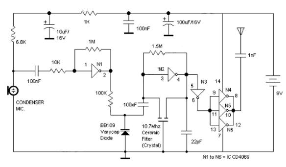
Logic Gates FM Transmitter Circuit
Logic Gates FM Transmitter Circuit Electronic Circuit Schematic Wiring Diagram.
The FM transmitter circuit utilizing logic gates is a fundamental electronic design that operates by modulating a carrier frequency with an audio signal. This circuit typically consists of various logic gates...
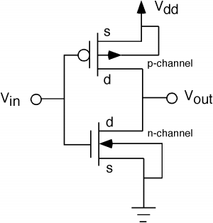
When abstract logic circuits get translated to the electrical equivilant how are conversions from 0 to 1 handled
The fundamental issue presented is the perception that logic gates in a circuit seem to generate power from nothing, which contradicts the principles of physics. For instance, consider two NOT gates connected in series. It appears that the first NOT...
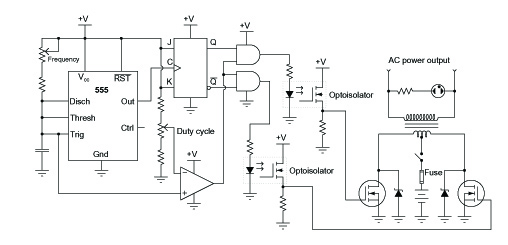
inverter circuit diagram
A common topology for DC-AC power converter circuits employs a pair of transistors to switch DC current through the center-tapped winding of a step-up transformer. Examine the check plot images from a PCB drafting program for a control board based...
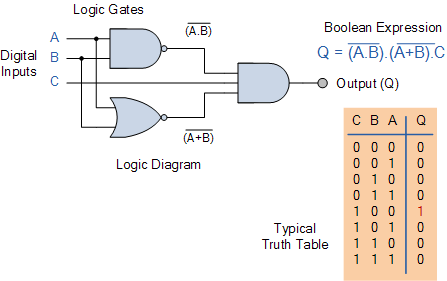
Combinational Logic Circuits using Logic Gates
Electronics tutorial on combinational logic circuits that utilize logic gates to create multiplexers, encoders, and solid-state switches.
Combinational logic circuits are fundamental components in digital electronics, characterized by their ability to produce outputs based solely on the current inputs, without any...
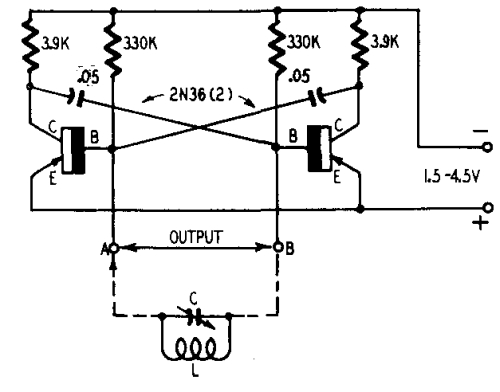
Oscillators and Triggers
Transistors are increasingly being utilized in various applications. Many circuits employing transistors have been developed based on previous designs that used vacuum tubes. The following chapters present unique applications that leverage the advantageous properties of transistors. The described circuits are...
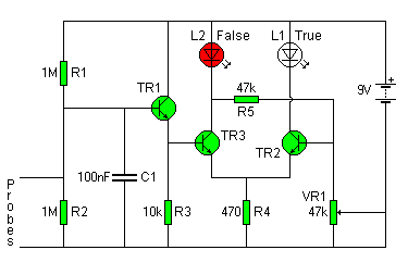
Lie detector
The circuit diagram of the Lie Detector is illustrated above. It consists of three transistors (TR1 to TR3), a capacitor (C1), two lights or LEDs (L1 & L2), five resistors (R1 to R5), and a variable resistor (VR1). This circuit...
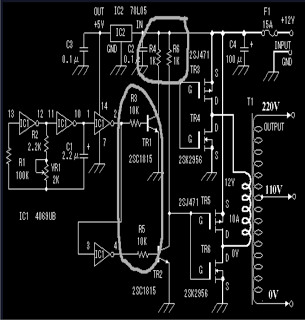
discussing output stage of square wave
The circuit includes 10K resistors at the bases of the transistors and 1K resistors at the collectors. It is essential to retain these components when relocating the transistors, as omitting the 10K resistors could result in transistor failure, and without...
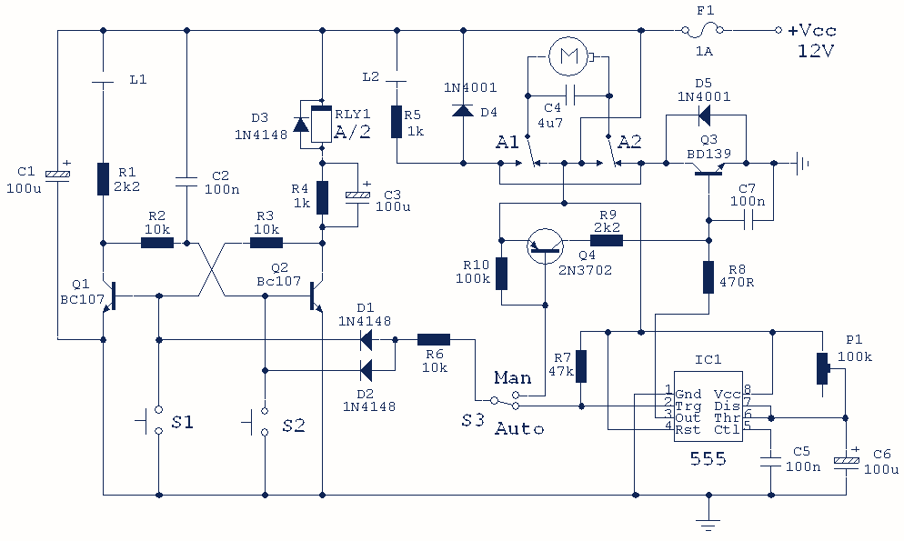
Curtain Control Circuit
This hybrid circuit uses a mixture of transistors, an IC and a relay and is used to automatically open or close a pair of curtains. Using switch S3 also allows manual control, allowing for curtains to be left only partially...
Logic Circuits Vs Transistor Power Circuits
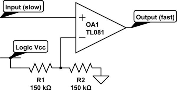
Invert a signal to drive FETs with rapid rise and fall times. It was suggested to use an inverter (not a chip) instead of logic chips, which are designed to be either fully ON or OFF. The individual has prior...