
home security system
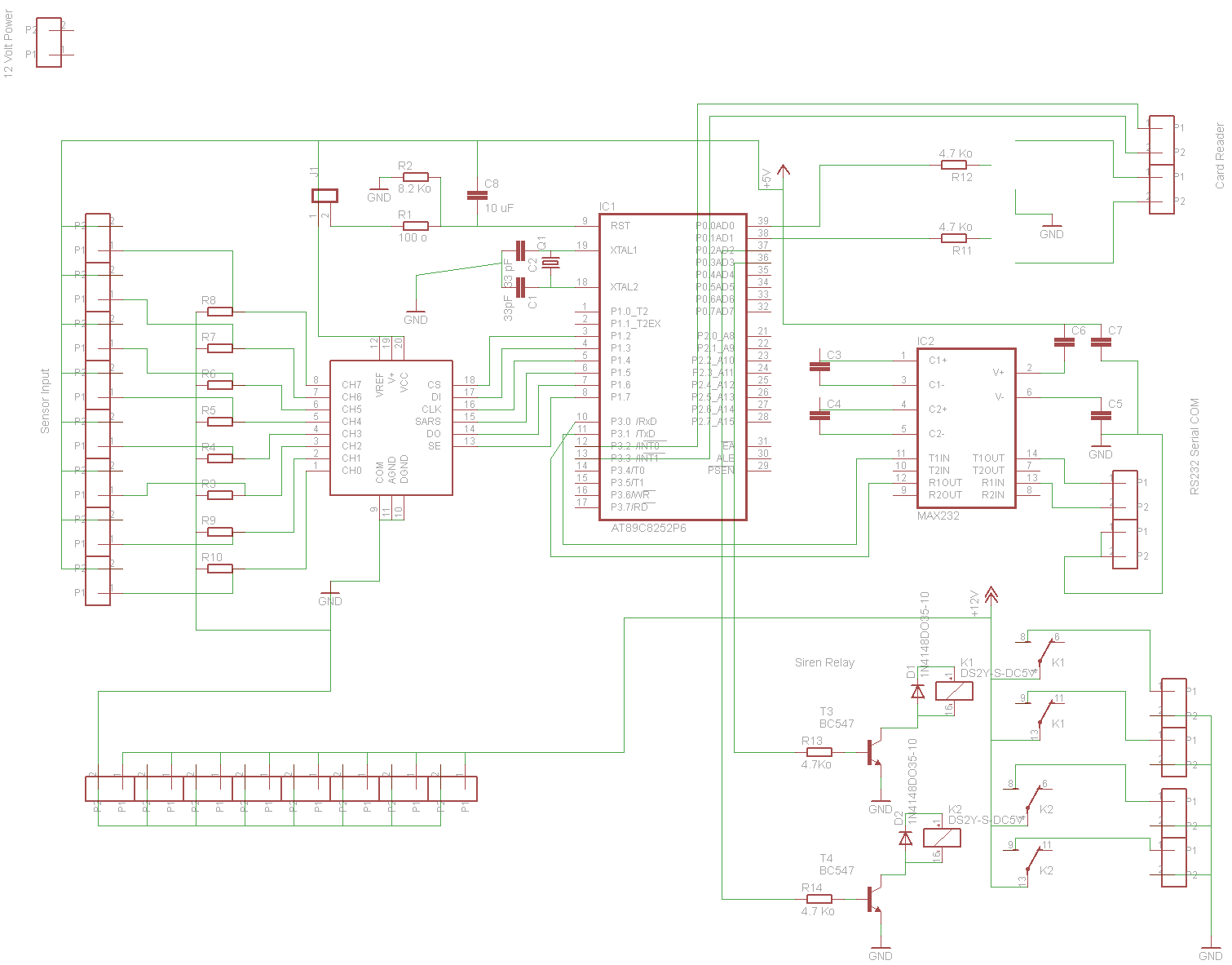
The circuit design integrates the Atmel AT89S8252-24PC microcontroller, which serves as the central processing unit for the system. This microcontroller is chosen for its sufficient EEPROM memory, allowing for temporary storage of sensor data and system states. The ADC0838CCN is connected to the microcontroller's analog input pins, enabling the conversion of analog signals from the sensors into digital data that the microcontroller can process.
In terms of security, the use of resistors in series with the sensors is a critical feature. This setup not only stabilizes the voltage levels but also provides a mechanism for fault detection. If an attempt is made to tamper with the wiring by cutting or shorting the sensor connections, the change in voltage levels will trigger an alarm condition.
The RFID system is an innovative approach to user authentication for arming and disarming the alarm. The HYE-01 Series LF Reader is interfaced with the microcontroller using the Wiegand protocol, which allows for efficient data transmission. The implementation of external interrupts (INT0 and INT1) is crucial for monitoring the Wiegand output lines. These interrupts are configured to trigger on the falling edge of the signals, enabling the microcontroller to accurately interpret the incoming data stream.
The timing mechanism for detecting the final bit of the Wiegand protocol is implemented using a timer module within the microcontroller. This ensures that the system can distinguish between the end of a data transmission and the start of a new one, maintaining the integrity of the data received.
Overall, this circuit design combines a microcontroller, ADC, and RFID technology to create a robust and secure alarm system capable of monitoring multiple sensor inputs while providing a user-friendly interface for system management.The basic design of this project will use a Atmel AT89S8252-24PC Microcontroller, since this micro has 2KB of EEPROM that can be used to store data during runtime. A ADC0838CCN analog to digital will be used to receive up to 8 inputs from sensor devices, such as PIR`s, reed switches, etc.
The reason behind using an ADC compared to just the DIO pin s is that it also adds some security by allowing resistors to be put inline to set the voltage to a specific level. If the wire to the sensor is cut or shorted, the alarm will be able to detect this occurring. To Arm/Disarm the system, an RFID tag reader will be used as apposed to a keypad. The chosen reader is a HYE-01 Series LF Reader that has both serial and Wiegand output. For this system the Wiegand output will be used to allow the serial connection to be used to connect to a computer.
When looking for information about the Wiegand protocol I found this page useful: The easy way of reading this data is to use the INT0 and INT1 external interrupts and configure them on the falling edge. This protocol works so that when DATA0 is low and DATA1 is high a 0 is produced and when DATA0 is high and DATA1 is low a 1 is produced.
In between bits both are high. The final bit is detected when both are high for 50ms, so a timer should also be used for detecting the final bit. 🔗 External reference
Related Circuits
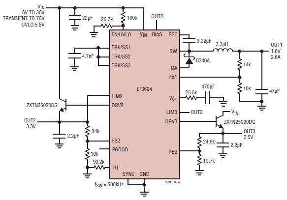
The LT3694 is a monolithic, current mode DC-DC converter that can be designed as a simple step-down converter, supporting a maximum output current of 2.6 A. This switching step-down converter is capable of generating up to 2.6 A at...
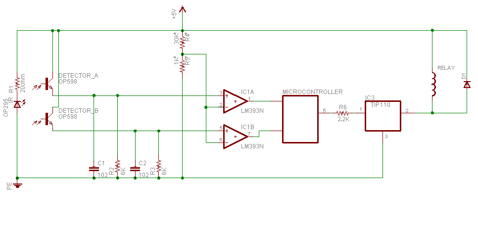
Sensing unit consists of infrared emitter OP295 to produce the infrared beam, and two detectors in front of the emitter to detect the infrared beam OP598. Since the main idea in this device is to know person direction; and...
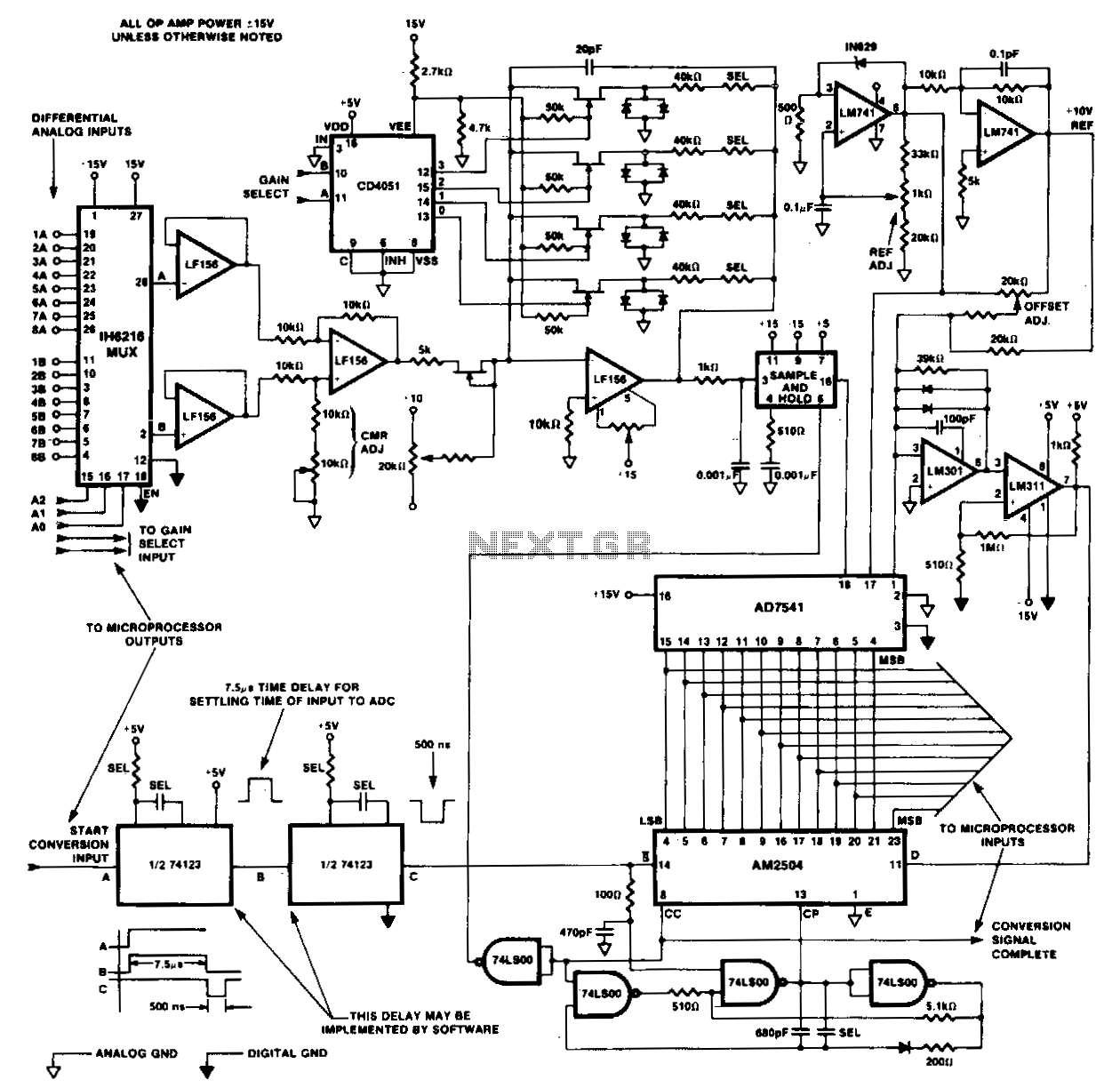
The front end of the DAC is configured differentially using dual eight-input IC multiplexer 1H6216 and three LM156 operational amplifiers. Following the differential amplifier is the programmable gain stage, which includes a low-pass filter on the output that feeds...
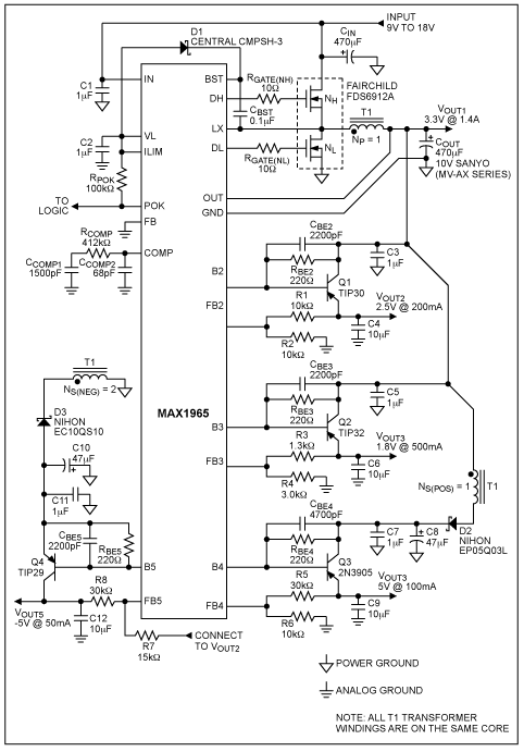
The power-supply controller features staggered voltage-output sequencing. Four voltage outputs are activated simultaneously for voltage tracking; two outputs are designated for core and I/O supplies during power-up, while the other two outputs cater to line driver supplies where tracking...
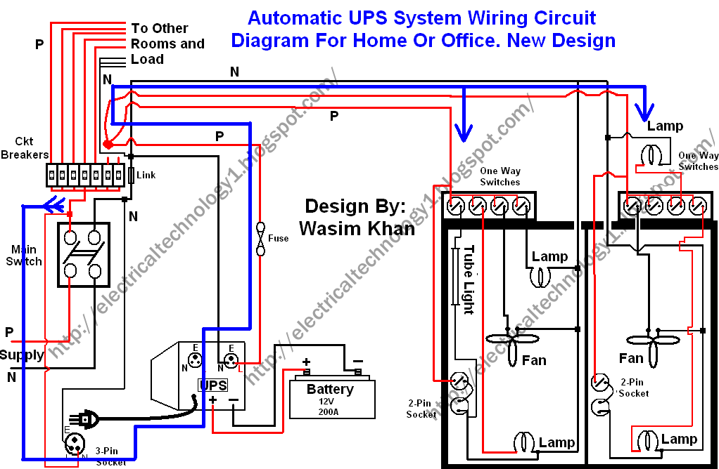
This wiring circuit diagram is designed for providing power to specific rooms in a home or office during a power supply failure. It ensures continuous power supply to devices such as laptops and computers in those particular rooms, especially...
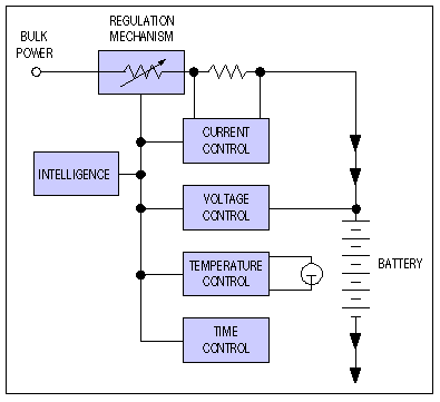
Application note on designing linear and switch-mode (switching DC-DC converter current source) battery charger applications that require external microcontrollers and related system-level issues for notebook computers. The application note provides guidance on the design of both linear and switching DC-DC...