


Composite-amplifier
#composite-amplifier
#HA-2539
#HA-2540
#wideband
#high-speed
#slew rate
#voltage gain
#bandwidth
#feedback
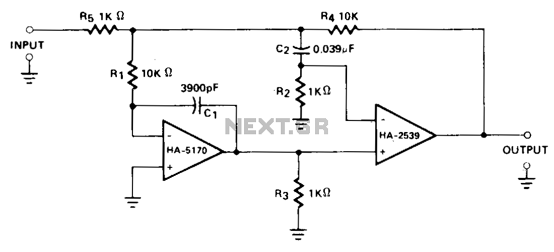
Description: A composite configuration significantly reduces errors without compromising the high-speed, wideband characteristics of the HA-2539. The HA-2540 can also be utilized, although it exhibits slightly lower speeds and bandwidth response. The HA-2539 amplifies signals above 40 kHz, which are forwarded via capacitor C2; resistors R2 and R5 establish a voltage gain of -10. The slew rate of this circuit is measured at 350 V/µs. The settling time to a 0.1% level for a 10-V output step is under 150 ns, and the gain bandwidth product is 300 MHz. The HA-5170 amplifies signals below 40 kHz, as determined by capacitor C1 and resistor R1, and manages the DC input characteristics such as offset voltage, drift, and bias currents of the composite amplifier. It features an offset voltage of 100 µV, a drift of 2 µV/°C, and bias currents in the 20 pA range. The offset voltage can be externally nulled by connecting a 20 kΩ potentiometer to pins 1 and 5, with the wiper connected to the negative supply. The DC gains of the HA-5170 and HA-2539 are cascaded, resulting in a composite amplifier DC gain of well over 160 dB. The outstanding AC and DC performance of this composite amplifier is further enhanced by its low noise performance, measuring 0.5 µV RMS from 0.1 Hz to 100 Hz. This configuration is particularly beneficial in high-speed data acquisition systems.
The composite amplifier circuit utilizes the HA-2539 and HA-5170 operational amplifiers to achieve high-performance signal amplification across a wide frequency range. The HA-2539 is specifically designed for high-frequency applications, amplifying signals above 40 kHz. The configuration employs capacitors and resistors to set the gain and manage signal integrity. Capacitor C2 plays a crucial role in coupling the amplified signal while resistors R2 and R5 are configured to establish a negative voltage gain of -10, which inversely amplifies the input signal, thus enhancing the output signal's amplitude while maintaining signal fidelity.
The HA-5170, on the other hand, is optimized for low-frequency signals below 40 kHz. Its role in the composite setup is critical for managing DC characteristics, such as offset voltage and drift, which can adversely affect signal accuracy. The offset voltage of 100 µV and drift rate of 2 µV/°C indicate the precision of the amplifier, making it suitable for applications that require high stability over temperature variations. The bias current of 20 pA ensures minimal loading on the signal source, preserving the integrity of the input signal.
In practical applications, the offset voltage can be adjusted externally using a potentiometer, allowing for fine-tuning of the amplifier's performance to meet specific requirements. The cascading of gains between the HA-5170 and HA-2539 results in an overall DC gain exceeding 160 dB, which is advantageous for applications requiring significant amplification of weak signals.
The low noise performance of the composite amplifier, quantified at 0.5 µV RMS from 0.1 Hz to 100 Hz, is a critical parameter for high-speed data acquisition systems. This low noise level ensures that the signal-to-noise ratio remains favorable, thus enhancing the quality of the acquired data. The combination of high-speed operation, wide bandwidth, and low noise makes this composite amplifier configuration ideal for applications in telecommunications, instrumentation, and any system where accurate signal processing is paramount.A composite configuration greatly reduces de errors without compromising the high-speed, wideband characteristics of HA-2539. The HA-2540 could also be used, but with slightly lower speeds and bandwidth response. The HA-2539 amplifies signals above 40 kHz which are fed forward via C2; R2 and R5 set the voltage gain at -10.
The slew rate of this circuit was measured at 350 V /p.s. Settling time to a 0.1 % level for a 10-V output step is under 150 ns and the gain bandwidth product is 300 MHz. The HA-5170 amplifies signals below 40kHz, as set by C1 and R1, and controls the de input characteristics such as offset voltage, drift, and bias currents of the composite amplifier. Therefore, it has an offset voltage ofl00 p.V, drift of 2 p.V/°C, and bias currents in the 20-pA range.
The offset voltage can be externally nulled by connecting a 20-KO pot to pins 1 and 5; with the wiper tied to the negative supply. The de gains of the HA-5170 and HA-2539 are cascaded; this means that the de gain of the composite amplifier is well over 160 dB.
The excellent ac and de performance of this composite amplifier is complemented by its low noise performance, 0.5-p. V rms from 0.1 Hz to 100Hz. It is very useful in high-speed data acquisition systems.
The composite amplifier circuit utilizes the HA-2539 and HA-5170 operational amplifiers to achieve high-performance signal amplification across a wide frequency range. The HA-2539 is specifically designed for high-frequency applications, amplifying signals above 40 kHz. The configuration employs capacitors and resistors to set the gain and manage signal integrity. Capacitor C2 plays a crucial role in coupling the amplified signal while resistors R2 and R5 are configured to establish a negative voltage gain of -10, which inversely amplifies the input signal, thus enhancing the output signal's amplitude while maintaining signal fidelity.
The HA-5170, on the other hand, is optimized for low-frequency signals below 40 kHz. Its role in the composite setup is critical for managing DC characteristics, such as offset voltage and drift, which can adversely affect signal accuracy. The offset voltage of 100 µV and drift rate of 2 µV/°C indicate the precision of the amplifier, making it suitable for applications that require high stability over temperature variations. The bias current of 20 pA ensures minimal loading on the signal source, preserving the integrity of the input signal.
In practical applications, the offset voltage can be adjusted externally using a potentiometer, allowing for fine-tuning of the amplifier's performance to meet specific requirements. The cascading of gains between the HA-5170 and HA-2539 results in an overall DC gain exceeding 160 dB, which is advantageous for applications requiring significant amplification of weak signals.
The low noise performance of the composite amplifier, quantified at 0.5 µV RMS from 0.1 Hz to 100 Hz, is a critical parameter for high-speed data acquisition systems. This low noise level ensures that the signal-to-noise ratio remains favorable, thus enhancing the quality of the acquired data. The combination of high-speed operation, wide bandwidth, and low noise makes this composite amplifier configuration ideal for applications in telecommunications, instrumentation, and any system where accurate signal processing is paramount.A composite configuration greatly reduces de errors without compromising the high-speed, wideband characteristics of HA-2539. The HA-2540 could also be used, but with slightly lower speeds and bandwidth response. The HA-2539 amplifies signals above 40 kHz which are fed forward via C2; R2 and R5 set the voltage gain at -10.
The slew rate of this circuit was measured at 350 V /p.s. Settling time to a 0.1 % level for a 10-V output step is under 150 ns and the gain bandwidth product is 300 MHz. The HA-5170 amplifies signals below 40kHz, as set by C1 and R1, and controls the de input characteristics such as offset voltage, drift, and bias currents of the composite amplifier. Therefore, it has an offset voltage ofl00 p.V, drift of 2 p.V/°C, and bias currents in the 20-pA range.
The offset voltage can be externally nulled by connecting a 20-KO pot to pins 1 and 5; with the wiper tied to the negative supply. The de gains of the HA-5170 and HA-2539 are cascaded; this means that the de gain of the composite amplifier is well over 160 dB.
The excellent ac and de performance of this composite amplifier is complemented by its low noise performance, 0.5-p. V rms from 0.1 Hz to 100Hz. It is very useful in high-speed data acquisition systems.
Wideband-signal-splitter
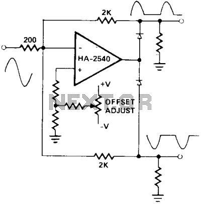
A circuit utilizing either the HA-2539 or HA-2540 in conjunction with two low-capacitance switching diodes can effectively separate signals exceeding 10 MHz. This configuration is particularly beneficial for applications such as full-wave rectification, AM detection, or synchronization generation.
The described circuit...
Wideband Active Rod Antenna
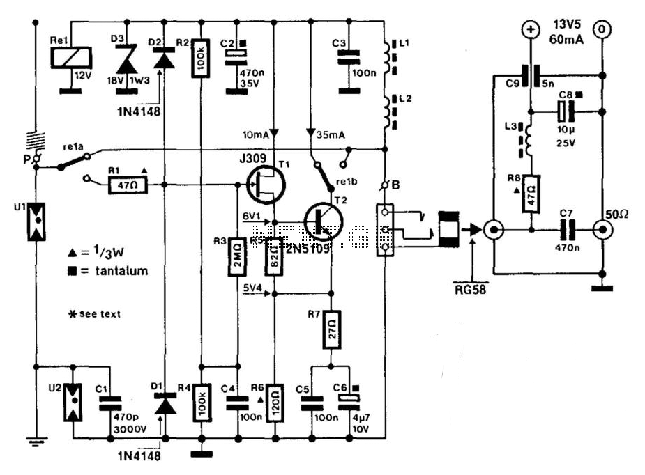
A J309 Siliconix FET is utilized to drive a 2N5109 in a wideband RF amplifier setup. A relay is incorporated to bypass the amplifier in transmit mode, if required. An active antenna element is a 2-meter 5/8-wave whip. The amplifier...
Wideband-500khz-1ghz-hybrid-amplifier
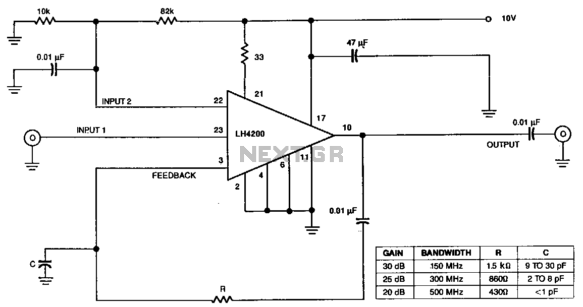
The amplifier's input stage features a dual-gate GaAs FET, which offers low input capacitance and high transconductance. The first input accepts the signal, while the second input regulates the amplifier's gain. Additionally, there is a third input for series feedback....
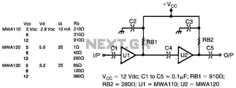
Wideband Preamp Circuit
Motorola MWA 110, 120, or 130 are wideband amplifier ICs. This wideband preamp circuit can be used in many applications. Keep the leads short when constructing the circuitry. PC board layout (shading represents copper) and parts layout. X is the...
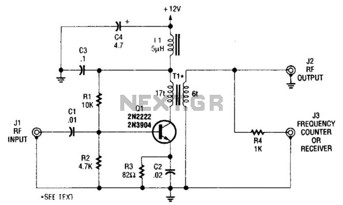
Wideband Test Amplifier
This single-stage amplifier, utilizing a 2N2222 or 2N3904 general-purpose transistor, is designed for interfacing with test instruments. The transformer T1 is an Amidon Associates FT-23-43 core, wound with 17 turns of #26 wire for the primary and 6 turns for...
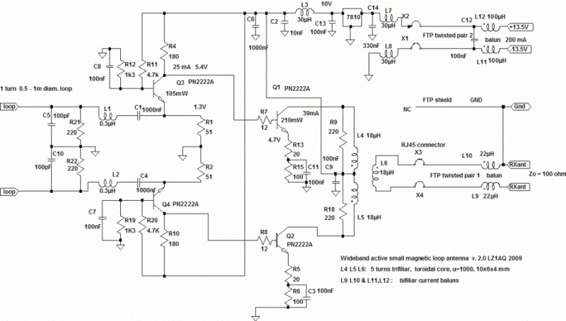
Wideband Active Small Magnetic Loop Antenna
There are extremely wideband software-defined radios (SDR) where a wideband antenna is a natural choice. Wideband small magnetic loops (WSM loops) have been used for 3-4 decades, and their effectiveness as a wideband SDR input is under evaluation. The WSM...
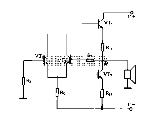
OCL yourself feedback amplifier analysis
The DC feedback circuit is illustrated in Figure 1-31. In this circuit, resistor R7 is connected to the output terminal, which is the midpoint of the static differential input stage voltage Vr, between the base terminals. This configuration represents a...
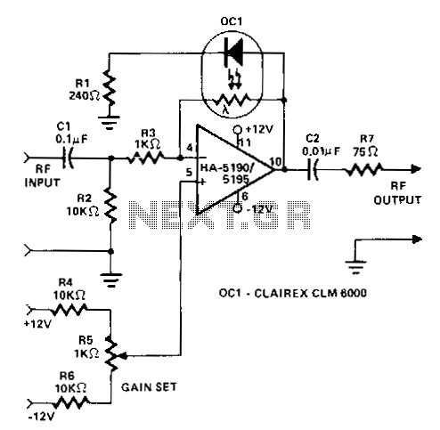
Rf-wideband-adjustable-agc-amplifier
This circuit operates as a wideband adjustable automatic gain control (AGC) amplifier. It has an effective bandwidth of approximately 10 MHz and can handle RF input signal frequencies ranging from 3.2 to 10 MHz at levels between 40 mV and...

Universal Wideband Amp
This kit is part of what is referred to as RF Tool Kits, specifically Electronic Building Blocks. A variety of these kits are available, with new ones being released periodically. The offerings can be explored and built in a homebrew...