


Rectification using a Gyrator Circuit
#rectification
#gyrator
#transistor
#capacitor
#2N3055
#ripple reduction
#current gain
#voltage regulation
#smoothing
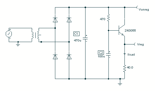
Description: To avoid excess ripple output on a power supply feeding a heavy load, usually a large value capacitor is chosen following the rectifier. In this circuit, C1 is only a 470uF capacitor. The gyrator principle uses the effect that the value of input capacitance at the base of a transistor is effectively multiplied by the current gain of the transistor. Here C2 which is 100u appears at the output (Vreg) to be 100 x current gain of the 2N3055 power transistor. If you assume a dc current gain of 50, then the smoothing across the supply would be as though you had chosen a 5000uF capacitor. The load draws nearly 400mA. With the output directly from the rectifier there is about 5V pk-pk ripple in the output. Using the output at the emitter of the transistor things are much better. The circuit will take a few hundred milliseconds for the
The described circuit employs a power supply configuration that minimizes output ripple by utilizing a combination of capacitors and a transistor following the rectification stage. Initially, a 470µF capacitor (C1) is connected post-rectification to smooth out the voltage fluctuations caused by the alternating current (AC) to direct current (DC) conversion. However, this value alone may not sufficiently reduce the ripple, especially under a load condition of 400mA.
To enhance the ripple suppression, the gyrator principle is employed, which leverages the current gain of a transistor—in this case, the 2N3055 power transistor. The gyrator acts as an effective capacitance multiplier. The capacitor C2, rated at 100µF, is placed at the output (Vreg) of the circuit. The effective capacitance at this node is significantly increased due to the transistor's current gain. Assuming a DC current gain (β) of 50 for the 2N3055, the output capacitance can be considered as being equivalent to a 5000µF capacitor. This multiplication of capacitance results in a much smoother voltage output, drastically reducing ripple.
The output from the rectifier exhibits approximately 5V peak-to-peak ripple when measured directly. However, by utilizing the emitter output of the 2N3055 transistor, the ripple is considerably lessened. This configuration allows the circuit to stabilize the output voltage more effectively, providing a cleaner DC supply to the load. The transient response of the circuit indicates that it may take several hundred milliseconds for the output voltage to stabilize after a load change or power-on condition, reflecting the time constant associated with the effective capacitance.
In summary, this circuit design efficiently reduces ripple in a power supply application by combining a rectifier, a strategically chosen capacitor, and a transistor utilizing the gyrator principle, resulting in a robust solution for powering heavy loads with minimal voltage fluctuation.To avoid excess ripple output on a power supply feeding a heavy load, usually a large value capacitor is chosen following the rectifier. In this circuit, C1 is only a 470uF capacitor. The gyrator principle uses the effect that the value of input capacitance at the base of a transitor is effectively multiplied by the current gain of the transistor.
Here C2 which is 100u appears at the ouput ( Vreg ) to be 100 x current gain of the 2N3055 power transistor. If you assume a dc current gain of 50, then the smoothing across the supply, would be as though you had chosen a 5000uF capacitor.
The load draws nearly 400mA. With the output directly from the rectifier there is about 5v pk-pk ripple in the output. Using the output at the emitter of the transistor things are much better. The circuit will take a few hundred milliseconds for the
The described circuit employs a power supply configuration that minimizes output ripple by utilizing a combination of capacitors and a transistor following the rectification stage. Initially, a 470µF capacitor (C1) is connected post-rectification to smooth out the voltage fluctuations caused by the alternating current (AC) to direct current (DC) conversion. However, this value alone may not sufficiently reduce the ripple, especially under a load condition of 400mA.
To enhance the ripple suppression, the gyrator principle is employed, which leverages the current gain of a transistor—in this case, the 2N3055 power transistor. The gyrator acts as an effective capacitance multiplier. The capacitor C2, rated at 100µF, is placed at the output (Vreg) of the circuit. The effective capacitance at this node is significantly increased due to the transistor's current gain. Assuming a DC current gain (β) of 50 for the 2N3055, the output capacitance can be considered as being equivalent to a 5000µF capacitor. This multiplication of capacitance results in a much smoother voltage output, drastically reducing ripple.
The output from the rectifier exhibits approximately 5V peak-to-peak ripple when measured directly. However, by utilizing the emitter output of the 2N3055 transistor, the ripple is considerably lessened. This configuration allows the circuit to stabilize the output voltage more effectively, providing a cleaner DC supply to the load. The transient response of the circuit indicates that it may take several hundred milliseconds for the output voltage to stabilize after a load change or power-on condition, reflecting the time constant associated with the effective capacitance.
In summary, this circuit design efficiently reduces ripple in a power supply application by combining a rectifier, a strategically chosen capacitor, and a transistor utilizing the gyrator principle, resulting in a robust solution for powering heavy loads with minimal voltage fluctuation.To avoid excess ripple output on a power supply feeding a heavy load, usually a large value capacitor is chosen following the rectifier. In this circuit, C1 is only a 470uF capacitor. The gyrator principle uses the effect that the value of input capacitance at the base of a transitor is effectively multiplied by the current gain of the transistor.
Here C2 which is 100u appears at the ouput ( Vreg ) to be 100 x current gain of the 2N3055 power transistor. If you assume a dc current gain of 50, then the smoothing across the supply, would be as though you had chosen a 5000uF capacitor.
The load draws nearly 400mA. With the output directly from the rectifier there is about 5v pk-pk ripple in the output. Using the output at the emitter of the transistor things are much better. The circuit will take a few hundred milliseconds for the
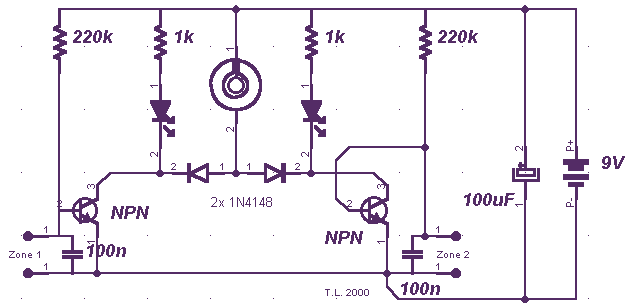
Miniature Loop Alarm
Simple construction, reliable operation, very small power consumption, and, most of all, small size. I started with CMOS logic gates, but was soon forced to abandon the concept after a few unsuccessful (and far too complicated) attempts. Then I suddenly...
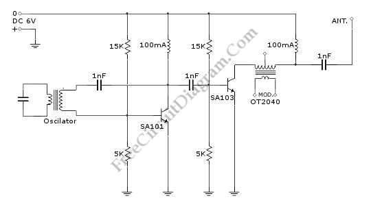
2 Transistors Mini MW Transmitter
This is a Mini MW (Medium Wave) Transmitter circuit. This circuit consists of a combination of transistors SA103 and SA101. These transistors are used as oscillators.
The Mini MW Transmitter circuit is designed to operate in the medium wave band, typically...
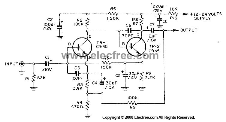
Dynamic Microphone Preamplifier using C945 transistor
This circuit utilizes three transistors (2SC945, 2C1815, or 2SC828) as the primary components, functioning as a typical low-noise transistor amplifier. It offers a gain of approximately 200 to 300 times and has a frequency response ranging from 50Hz to 100KHz....
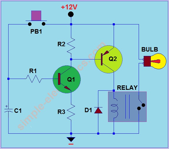
Car Headlight with Delay Circuit
This circuit operates by activating a headlight when the push-button PB1 is pressed. The headlight remains illuminated for a predetermined duration, which can range from several seconds to minutes, before automatically turning off. When PB1 is engaged, capacitor C1 begins...
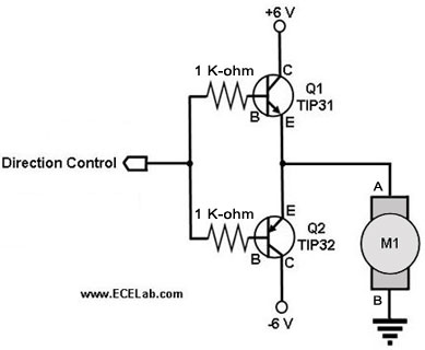
Two-Transistor DC Motor DriverCircuit Using The TIP32 Transistor
The following circuit illustrates a two-transistor DC motor driver circuit diagram. This circuit utilizes the TIP32 transistor. Features: operates in...
The two-transistor DC motor driver circuit is designed to control the operation of a DC motor using two NPN transistors, which...
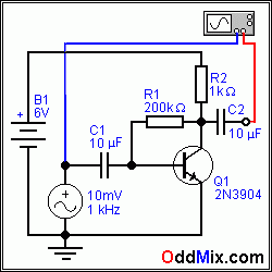
transistor amplifier self bias
The simplest way to bias a transistor amplifier is through a fixed-bias circuit. The supply voltage is connected to the base terminal of the transistor via the R1 current-limiting resistor. The bias resistor value is typically chosen based on the...
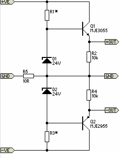
Simple Pre-Regulator
There will be many occasions when it is beneficial to utilize the P05 supply module sourced from a higher voltage supply. For instance, this could be advantageous when integrating balanced inputs.
The P05 supply module is designed to facilitate the conversion...
Water Activated Relay
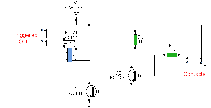
In this circuit, two transistors are configured as a high-gain compound pair. Transistor T1 is likely a 2N2222A, while T2 is identified as a BC108. The current gain is calculated as the product of the beta values of each transistor,...
ISO107 ripple reduction circuit
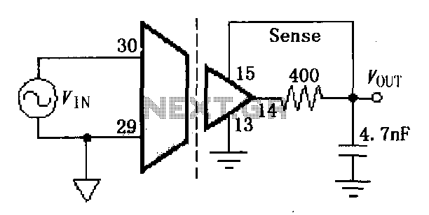
The ISO107 ripple reduction circuit includes an RC high-pass filter at the output to filter the output voltage ripple without impacting the DC characteristics. This configuration allows for a reduction of the 800kHz ripple voltage to less than 3mVp-p.
The ISO107...