


Ultra Small Mobile Phone Xenon Photoflash Capacitor Charger With IGBT Driver
#capacitor charger
#IGBT driver
#step-up regulator
#evaluation board
#voltage regulation
#output current
#AAT1265
#low voltage
#2MHz
#external components
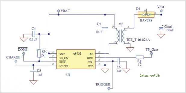
Description: The AAT1265 evaluation board serves as a platform for testing and evaluating the AAT1265 low voltage 2MHz step-up regulator. This evaluation board illustrates the recommended size and arrangement of external components necessary to maintain output voltage regulation for up to 250mA of output current. The selected external components are designed for compactness to suit portable applications, while the layout has been optimized to achieve high efficiency with the SC70JW-8 package. The design operates over an input voltage range of 0.8V to VOUT. The AAT1265 evaluation demo board provides a 3.3V output at a maximum output current of 250mA for a dual AA cell input. This document outlines the operation and testing procedures for the AAT1265 evaluation board.
The AAT1265 evaluation board is engineered to facilitate the assessment of the AAT1265 low voltage step-up converter, which operates at a frequency of 2MHz. The board's design is crucial for maintaining voltage regulation while sourcing up to 250mA of output current, making it suitable for various portable electronic applications. The external components, including inductors and capacitors, are meticulously chosen for their small footprint, ensuring that the overall design remains compact and efficient.
The layout of the evaluation board is optimized to minimize parasitic inductance and resistance, which can adversely affect performance. This optimization is particularly important in high-frequency applications where switching losses can significantly impact efficiency. The use of the SC70JW-8 package further enhances the board's space efficiency, allowing for integration into compact devices.
The input voltage range of 0.8V to VOUT enables the board to operate effectively with low-voltage power sources, such as dual AA batteries, making it versatile for battery-operated devices. The specified output voltage of 3.3V is a standard requirement for many digital circuits, ensuring compatibility with a wide range of applications.
Operational testing of the AAT1265 evaluation board involves monitoring the output voltage and current under various load conditions to verify the regulator's performance. The evaluation board also provides test points for measuring input and output voltages, as well as current monitoring, facilitating comprehensive performance analysis.
In summary, the AAT1265 evaluation board is a well-designed tool for engineers and developers looking to evaluate the performance of the AAT1265 step-up regulator in portable applications, ensuring that both design and testing processes are streamlined and efficient.The AAT1265 evaluation board provides a platform for the testing and evaluation of the AAT1265 low voltage 2MHz Step-up Regulator The evaluation board demonstrates suggested size and placement of external components to main- tain output voltage regulation for up to 250mA of output current. The external components are selected for small size to sui t portable applications while the layout has been optimized to achieve high efficiency with the SC70JW-8 package. The design operates across an input voltage range of 0. 8V to VOUT. The AAT1265 EVAL demo board provides a 3. 3V output at 250mA maximum output current for a dual AA cell input. This document provides details on the operation and testing of the AAT1265 evaluation board. AAT1265IJS Low Voltage 2MHz Step-up Converter
The AAT1265 evaluation board is engineered to facilitate the assessment of the AAT1265 low voltage step-up converter, which operates at a frequency of 2MHz. The board's design is crucial for maintaining voltage regulation while sourcing up to 250mA of output current, making it suitable for various portable electronic applications. The external components, including inductors and capacitors, are meticulously chosen for their small footprint, ensuring that the overall design remains compact and efficient.
The layout of the evaluation board is optimized to minimize parasitic inductance and resistance, which can adversely affect performance. This optimization is particularly important in high-frequency applications where switching losses can significantly impact efficiency. The use of the SC70JW-8 package further enhances the board's space efficiency, allowing for integration into compact devices.
The input voltage range of 0.8V to VOUT enables the board to operate effectively with low-voltage power sources, such as dual AA batteries, making it versatile for battery-operated devices. The specified output voltage of 3.3V is a standard requirement for many digital circuits, ensuring compatibility with a wide range of applications.
Operational testing of the AAT1265 evaluation board involves monitoring the output voltage and current under various load conditions to verify the regulator's performance. The evaluation board also provides test points for measuring input and output voltages, as well as current monitoring, facilitating comprehensive performance analysis.
In summary, the AAT1265 evaluation board is a well-designed tool for engineers and developers looking to evaluate the performance of the AAT1265 step-up regulator in portable applications, ensuring that both design and testing processes are streamlined and efficient.The AAT1265 evaluation board provides a platform for the testing and evaluation of the AAT1265 low voltage 2MHz Step-up Regulator The evaluation board demonstrates suggested size and placement of external components to main- tain output voltage regulation for up to 250mA of output current. The external components are selected for small size to sui t portable applications while the layout has been optimized to achieve high efficiency with the SC70JW-8 package. The design operates across an input voltage range of 0. 8V to VOUT. The AAT1265 EVAL demo board provides a 3. 3V output at 250mA maximum output current for a dual AA cell input. This document provides details on the operation and testing of the AAT1265 evaluation board. AAT1265IJS Low Voltage 2MHz Step-up Converter
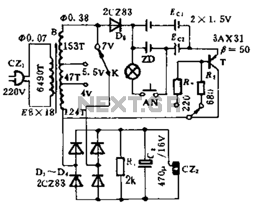
Low voltage DC power charger circuit
This circuit is designed for high current applications using nickel-cadmium rechargeable batteries, and it can also function as a general low-voltage DC power supply. The circuit consists of a charging section and a DC output section. K2 serves as the...
Voltage Regulators
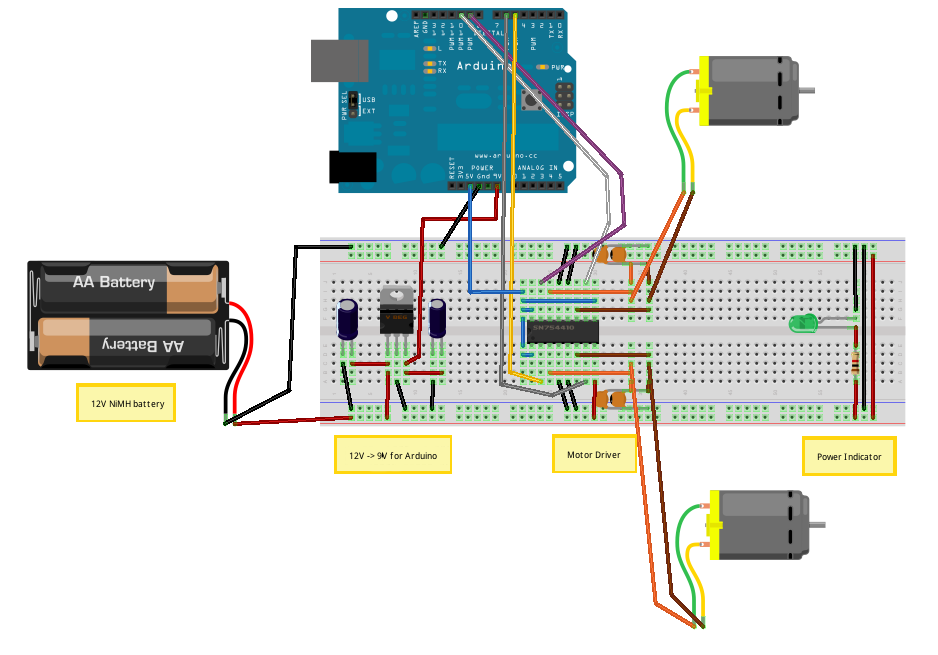
Until Willow Garage was acquired, there was work as a Web Robotics Engineer. This title reflects a role as a full-stack engineer focused on real-time, distributed robot control. Notable projects include an XML-RPC server and client for Node.js, a deprecated...
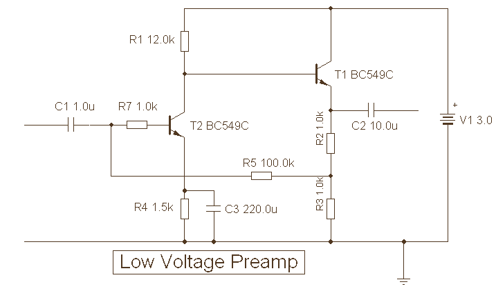
Low Voltage Preamplifier
The provided description pertains to a unique low voltage variant of an audio preamp. The emitter voltage of T1 is biased close to half the supply voltage, which is 1.5V. This biasing allows for the maximum output voltage swing. The...
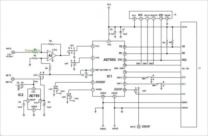
Evaluation Board For Single Supply 12-bit 500 Ksps Adc
This data sheet describes the evaluation board for the AD9834 direct digital synthesizer (DDS). The AD9834 is a numerically controlled oscillator that utilizes a phase accumulator, a sine look-up table, and a 10-bit DAC. The AD9834 can operate with clock...
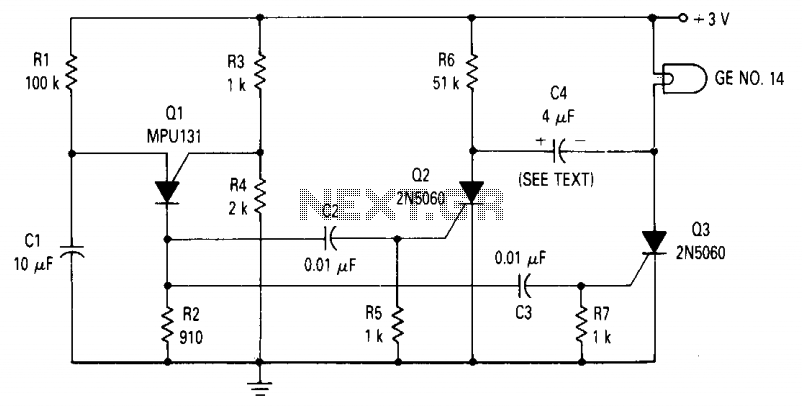
Low voltage lamp flasher
The circuit consists of a relaxation oscillator created by Q1 and an SCR flip-flop formed by Q2 and Q3. When the supply voltage is applied to the circuit, the timing capacitor C1 charges to the firing point of the Programmable...
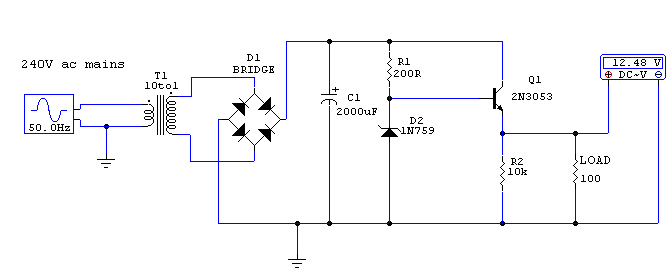
Regulated 12 Volt Supply
This circuit utilizes a 13-volt zener diode (D2) for voltage regulation. Approximately 0.7 volts are dropped across the base-emitter junction of the transistors, resulting in a higher current output of 12.3 volts. The circuit is capable of supplying loads up...
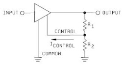
Voltage Regulator
Neither term describes a regulator, only its placement within a circuit or system. Any voltage regulator could meet the requirements, depending on its placement. A listing of Analog Voltage Regulator IC manufacturers. The types of products or devices they produce...
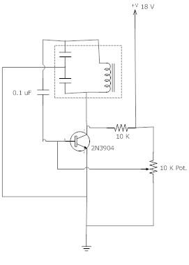
Simple low voltage Oscillator circuit
The frequency remains stable as the voltage decreases. It is referred to as the "backwards JT" because it operates optimally with a bifilar coil and a single transistor. With a modification to the circuit, it is possible to deplete a...
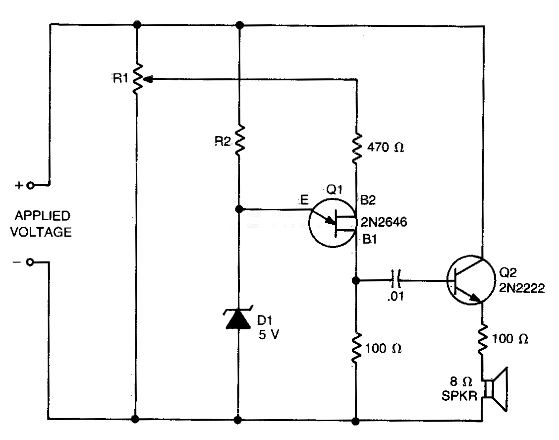
Low voltage detector
The values of R1, R2, and D1 are selected based on the voltage applied. Using a 12-volt battery, R1 is set to 10 kΩ, R2 to 5 kΩ, and D1 is a 5-volt zener diode or a string of forward-biased...