


Switch-Mode Voltage Regulator
#switch-mode
#power supply
#voltage regulation
#efficiency
#DC-DC converter
#PWM
#step-down
#step-up
#buck-boost
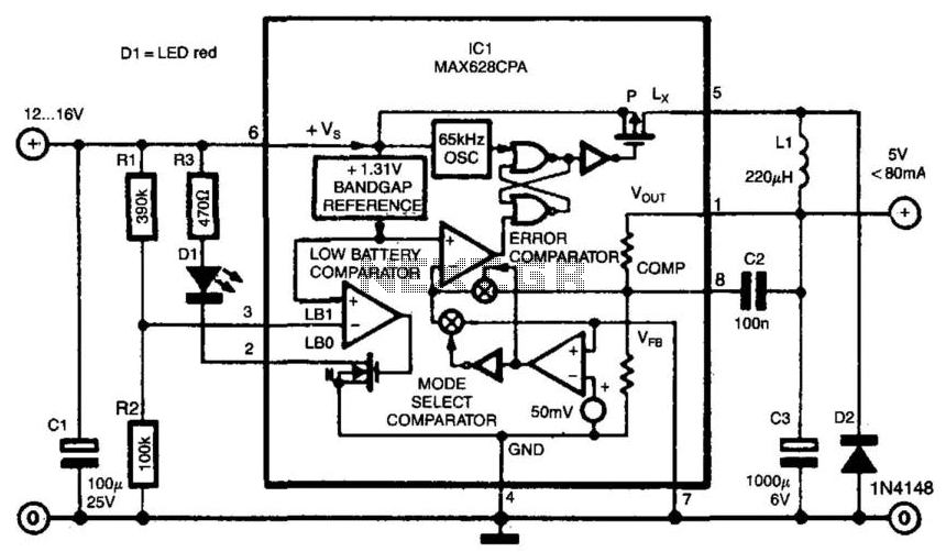
Description: Switch-mode power supplies offer significantly greater efficiency compared to traditional power supplies. The switch-mode regulator described here achieves an efficiency of approximately 85%. It converts an input voltage range of 12 to 16 VDC into a stable output voltage of 5 V. The design utilizes a MAX638CPA, allowing for a relatively simple circuit with only nine additional components required for completion. Resistors R1 and R2 serve as indicators for low battery voltage; when the voltage on pin 3 drops below 1.3 V, diode D1 illuminates. With the specified values for the potential divider, this indicates that the supply voltage has fallen below approximately 6.5 V. The output of the integrated circuit (IC) is filtered using a simple LC filter composed of inductor L1, capacitor C3, and diode D2. The IC features an onboard oscillator that generates a clock frequency of around 65 kHz, which drives the output transistor through two NOR gates. The integrated error detector, low battery indicator, and voltage comparator can disable the clock frequency, causing the transistor to turn off. The IC compares the output voltage of 5 V with an internal reference (FET), adjusting the FET's on-time based on the load conditions. The maximum current through the FET is 375 mA, allowing for a maximum output current of 80 mA.
The switch-mode power supply circuit is designed to optimize efficiency while providing reliable voltage regulation. The MAX638CPA integrated circuit serves as the core of the regulator, facilitating the conversion process with minimal external components. The choice of components is critical; for instance, the inductor L1 and capacitor C3 form a low-pass LC filter that smooths out the output voltage, ensuring that the 5 V supply is stable and free from high-frequency noise generated during the switching process.
The feedback mechanism is crucial for maintaining the desired output voltage. The internal error detector continuously monitors the output voltage and compares it to a precise reference voltage. If the output voltage deviates from the specified 5 V, the FET is modulated to adjust the energy transfer to the load, thereby maintaining regulation. This feedback loop is essential for adapting to varying load conditions, ensuring that the output remains consistent under different operational scenarios.
The low battery indicator feature enhances the usability of the power supply by providing a visual alert when the input voltage approaches a critical threshold. This is particularly useful in battery-powered applications where monitoring the battery state is essential for preventing unexpected shutdowns.
Overall, this switch-mode power supply design exemplifies a balance of efficiency, simplicity, and functionality, making it suitable for various applications where reliable voltage regulation is required. The careful selection of components and the integrated features of the MAX638CPA contribute to the overall performance and reliability of the circuit. Switch-mode power supplies offer the benefit of a much greater efficiency than obtainable with a traditional power supply. The switch-mode regulator presented here has an efficiency of around 85%. An input voltage of 12 to 16 Vdc is converted into a direct voltage of exactly 5 V. The use of a MAX638CPA enables the design and construction of the regulator to be kept fairly simple: only nine additional components are needed to complete the circuit. Resistors RI and R2 are used to indicate when the battery voltage becomes low: as soon as the voltage on pin 3 becomes lower than 1.3 V, D1 lights.
With values as shown for the potential divider, this corresponds to the supply voltage getting lower than about 6.5 V. The output of the IC is shunted by a simple LC filter formed by LI, C3 and D2. The oscillator on board the IC generates a clock frequency of around 65 kHz and drives the output transistor via two NOR gates.
The built-in error detector, the "battery low" indicator or the voltage comparator can block the clock frequency, which causes the transistor to switch off. The IC compares the output voltage of 5 V with a built-in reference (FET). Depending on the load, the FET will be switched on for longer or shorter periods. The maximum current through the FET is 375 mA, which corresponds with a maximum output current of 80 mA.
The switch-mode power supply circuit is designed to optimize efficiency while providing reliable voltage regulation. The MAX638CPA integrated circuit serves as the core of the regulator, facilitating the conversion process with minimal external components. The choice of components is critical; for instance, the inductor L1 and capacitor C3 form a low-pass LC filter that smooths out the output voltage, ensuring that the 5 V supply is stable and free from high-frequency noise generated during the switching process.
The feedback mechanism is crucial for maintaining the desired output voltage. The internal error detector continuously monitors the output voltage and compares it to a precise reference voltage. If the output voltage deviates from the specified 5 V, the FET is modulated to adjust the energy transfer to the load, thereby maintaining regulation. This feedback loop is essential for adapting to varying load conditions, ensuring that the output remains consistent under different operational scenarios.
The low battery indicator feature enhances the usability of the power supply by providing a visual alert when the input voltage approaches a critical threshold. This is particularly useful in battery-powered applications where monitoring the battery state is essential for preventing unexpected shutdowns.
Overall, this switch-mode power supply design exemplifies a balance of efficiency, simplicity, and functionality, making it suitable for various applications where reliable voltage regulation is required. The careful selection of components and the integrated features of the MAX638CPA contribute to the overall performance and reliability of the circuit. Switch-mode power supplies offer the benefit of a much greater efficiency than obtainable with a traditional power supply. The switch-mode regulator presented here has an efficiency of around 85%. An input voltage of 12 to 16 Vdc is converted into a direct voltage of exactly 5 V. The use of a MAX638CPA enables the design and construction of the regulator to be kept fairly simple: only nine additional components are needed to complete the circuit. Resistors RI and R2 are used to indicate when the battery voltage becomes low: as soon as the voltage on pin 3 becomes lower than 1.3 V, D1 lights.
With values as shown for the potential divider, this corresponds to the supply voltage getting lower than about 6.5 V. The output of the IC is shunted by a simple LC filter formed by LI, C3 and D2. The oscillator on board the IC generates a clock frequency of around 65 kHz and drives the output transistor via two NOR gates.
The built-in error detector, the "battery low" indicator or the voltage comparator can block the clock frequency, which causes the transistor to switch off. The IC compares the output voltage of 5 V with a built-in reference (FET). Depending on the load, the FET will be switched on for longer or shorter periods. The maximum current through the FET is 375 mA, which corresponds with a maximum output current of 80 mA.
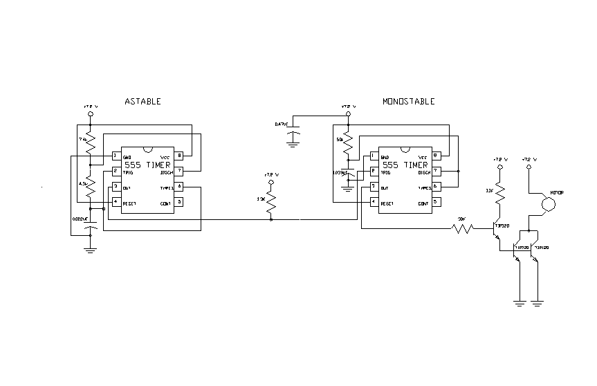
pulse width modulated (PWM) controller for high current
The second 555 timer was configured as a monostable circuit, commonly referred to as a one-shot since an output pulse only occurs if there is a trigger on the input. When this timer is triggered, the potentiometer in the RC...
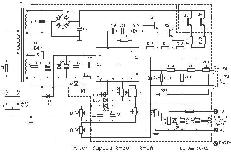
Power Supply 0-30V / 0-2A
The basic requirements for a laboratory power supply are to provide the necessary voltages and currents with low output resistance, low noise, minimal ripple, and good stabilization. These requirements are addressed within the circuit design. Many power supplies incorporate electronic...
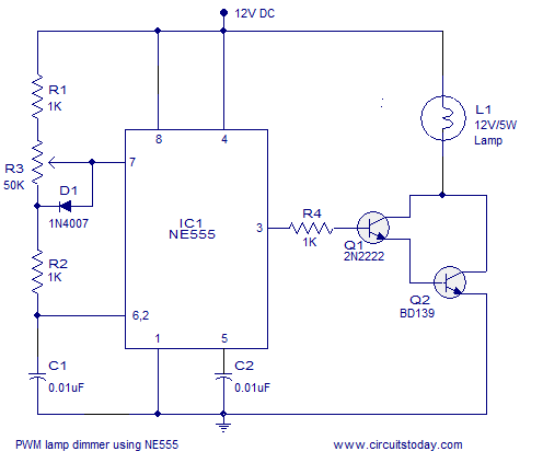
PWM lamp dimmer using NE555 timer IC. Complete circuit diagram and working
A simple PWM lamp dimmer using the NE555 timer IC. The 555 timer IC is configured as a variable duty cycle astable multivibrator to control the brightness of the lamp.
The described circuit utilizes the NE555 timer IC, a versatile and...
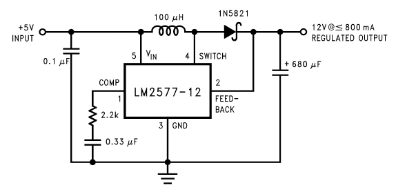
LM2577 5V to 12V DC Converter step up Voltage Regulator
If you are looking for ICs for a DC to DC converter application, the LM1577/LM2577 ICs are highly recommended as they provide all the necessary power and control functions for step-up conversion.
The LM1577 and LM2577 are versatile integrated circuits designed...
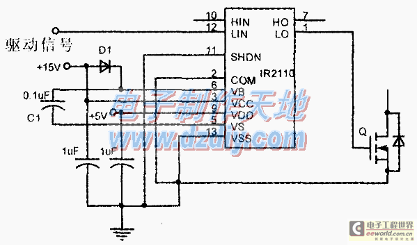
Design and making of the stabilized voltage supply of switch
Under the loading condition of the resistance, the output voltage (Uo) variable range is from 30V to 36V, with a maximum output current (Imax) of 2A. When the input voltage (U2) changes from 15V to 21V, the voltage regulation factor...
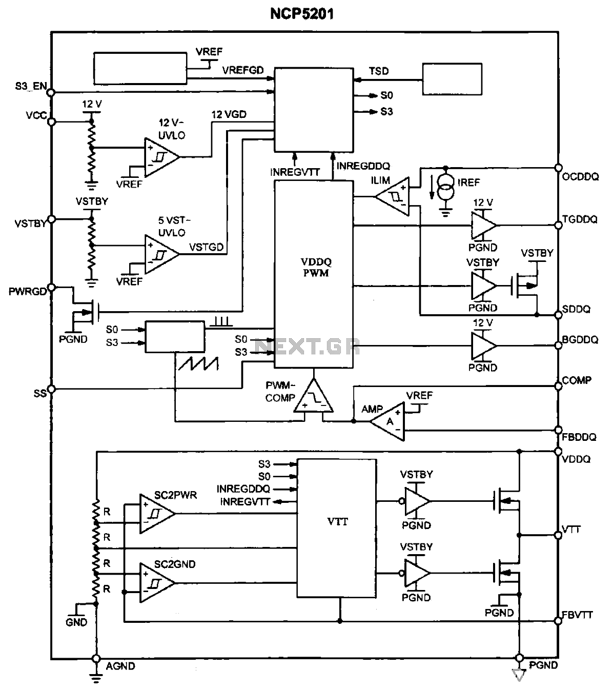
Internal functional block diagram of NCP5201
The NCP5201 chip contains two sets of PWM signal generating circuits, each with a dedicated set of output pins. These circuits produce two opposite phase PWM signals, which are applied to the gates of three field effect transistors. This arrangement...
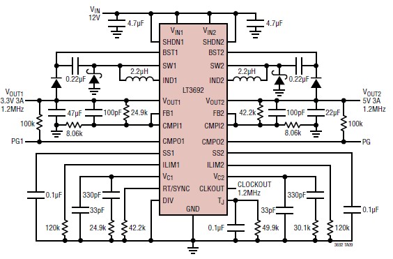
3.3V and 5V DC DC converter circuit design using LT3692 DC converter dual tracking regulator
The LT3692 dual current mode PWM step-down DC-DC converter circuit, featuring two internal 3.5A switches, can be designed into a simple power supply circuit suitable for various electronic applications, such as distributed supply regulation or automotive circuits. The LT3692 provides...
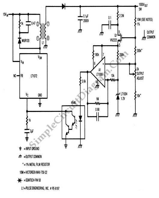
Isolated 15 to 1000V DC-DC Converter
The circuit illustrated in the schematic diagram below is an isolated DC-to-DC step-up converter. The term "isolated" indicates that there is no electrical connection between the input and output sections of the circuit.
The isolated DC-to-DC step-up converter operates by converting...
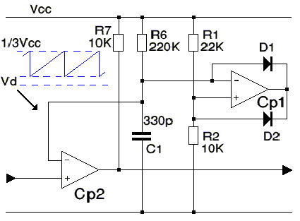
Levitation PWM
The switched controller utilized is effective; however, a pulse width modulation (PWM) circuit is more advantageous. It offers efficient operation with reduced heat generation and provides linear functioning. The implementation requires a minimal number of components. When capacitor C1 is...