


Voltage-mode control and compensation: Intricacies for buck regulators
#buck regulator
#voltage mode control
#compensation
#power electronics
#DC-DC converter
#control loop
#feedback
#switching regulator
#circuit design
#IC
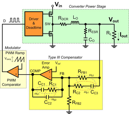
Description: Before designing with one of today's powerful buck regulator ICs, it is essential to have a thorough understanding of voltage mode control and compensation.
Voltage mode control is a widely used method in switching power supplies, particularly in buck converters. This technique regulates the output voltage by comparing it to a reference voltage and adjusting the duty cycle of the switching element accordingly. The control loop's stability and transient response are critical parameters that must be optimized to ensure reliable operation across varying load conditions.
Compensation in voltage mode control is necessary to achieve stable operation. It involves the design of a compensation network that shapes the frequency response of the control loop. Common compensation techniques include Type I, Type II, and Type III compensators, each offering different trade-offs in terms of phase margin, bandwidth, and transient response. The selection of the appropriate compensation scheme depends on the specific application requirements, load characteristics, and desired performance metrics.
When designing a buck converter, it is important to consider the following elements: input and output capacitors, inductor selection, diode characteristics, and PCB layout. Input capacitors must be chosen to handle the input voltage ripple, while output capacitors affect the output voltage ripple and transient response. Inductor selection impacts the efficiency and current ripple, and the diode must be rated for the expected current and voltage conditions.
Additionally, PCB layout plays a significant role in the performance of the buck converter. Proper grounding, trace widths, and component placement are crucial to minimize parasitic inductance and resistance, which can adversely affect the regulator's performance.
In summary, a comprehensive understanding of voltage mode control and compensation is vital for the effective design of buck regulator circuits. Proper selection of components and careful attention to layout will enhance the performance and reliability of the power supply design.Before designing with one of today`s powerful buck regulator ICs, you`ll want a thorough understanding of voltage mode control and compensation. ..
Voltage mode control is a widely used method in switching power supplies, particularly in buck converters. This technique regulates the output voltage by comparing it to a reference voltage and adjusting the duty cycle of the switching element accordingly. The control loop's stability and transient response are critical parameters that must be optimized to ensure reliable operation across varying load conditions.
Compensation in voltage mode control is necessary to achieve stable operation. It involves the design of a compensation network that shapes the frequency response of the control loop. Common compensation techniques include Type I, Type II, and Type III compensators, each offering different trade-offs in terms of phase margin, bandwidth, and transient response. The selection of the appropriate compensation scheme depends on the specific application requirements, load characteristics, and desired performance metrics.
When designing a buck converter, it is important to consider the following elements: input and output capacitors, inductor selection, diode characteristics, and PCB layout. Input capacitors must be chosen to handle the input voltage ripple, while output capacitors affect the output voltage ripple and transient response. Inductor selection impacts the efficiency and current ripple, and the diode must be rated for the expected current and voltage conditions.
Additionally, PCB layout plays a significant role in the performance of the buck converter. Proper grounding, trace widths, and component placement are crucial to minimize parasitic inductance and resistance, which can adversely affect the regulator's performance.
In summary, a comprehensive understanding of voltage mode control and compensation is vital for the effective design of buck regulator circuits. Proper selection of components and careful attention to layout will enhance the performance and reliability of the power supply design.Before designing with one of today`s powerful buck regulator ICs, you`ll want a thorough understanding of voltage mode control and compensation. ..
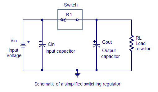
Few Switching regulator circuits
Switching regulators operate by drawing small amounts of energy from the input source and transferring it incrementally to the output. This is achieved using an electronic switch, which functions at a predetermined frequency, acting as a gate between the input...
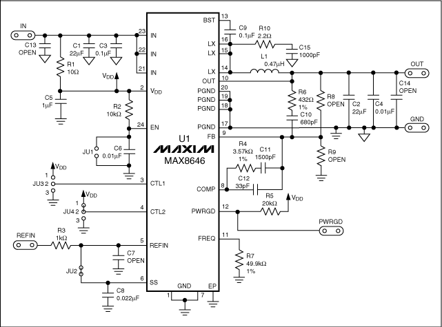
Inductor Choice Yields Performance Tradeoffs in DC-DC Converters
Cost, size, resistance, and current capability drive the choice of inductor for most step-down DC-DC switching converters.
Inductors play a crucial role in the operation of step-down DC-DC switching converters, influencing performance parameters such as efficiency, output voltage stability, and transient...
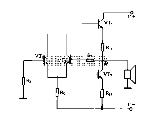
OCL yourself feedback amplifier analysis
The DC feedback circuit is illustrated in Figure 1-31. In this circuit, resistor R7 is connected to the output terminal, which is the midpoint of the static differential input stage voltage Vr, between the base terminals. This configuration represents a...
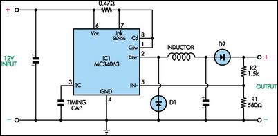
Cheap Switch-Mode DC-DC Converter
This circuit utilizes mobile phone chargers that incorporate the Motorola MC34063 switch-mode integrated circuit (IC). The output voltage can be adjusted across a broad spectrum by altering the values of the feedback resistors R1 and R2. The output voltage is...
Electronic Projects
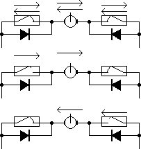
This program includes circuit design CAD, simulation, and auto-routing PC layout. PSPICE is also utilized at Unisys, which offers more capabilities but costs six times as much and requires annual renewal. With these requirements and others in mind, a variation...
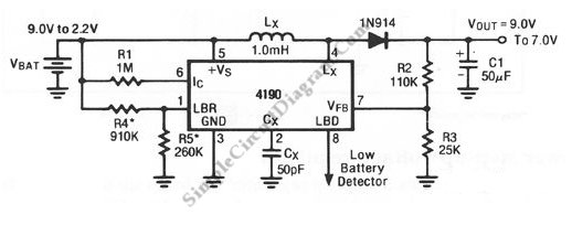
Extending Battery Life with Switching Regulator
A standard 9V battery is considered depleted when its voltage drops below 7 volts. This switching regulator can extend the lifetime of a 9V battery.
The circuit utilizes a switching regulator to optimize the energy usage of a standard 9V battery,...
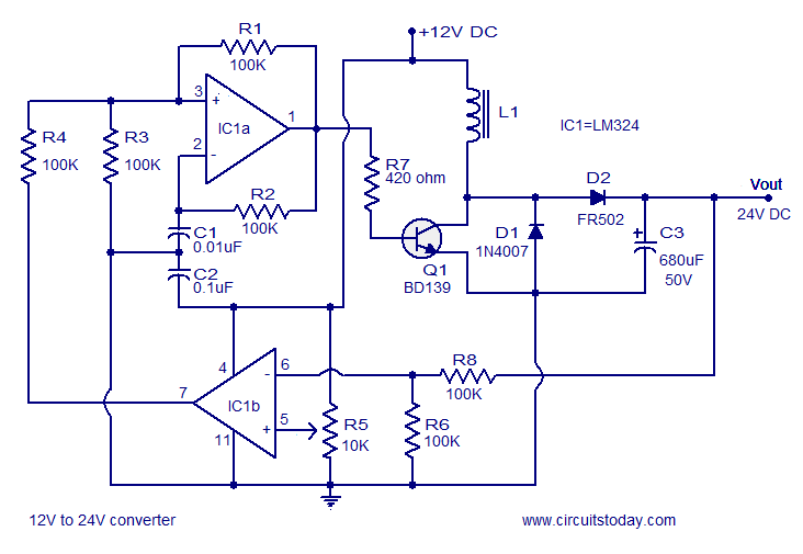
Simple 12V to 24V DC DC converter using LM324 and transistor
A simple 12V to 24V DC-DC converter circuit diagram built around the LM324. This boost converter schematic can provide up to 800mA output current and a steady 24V DC.
The described circuit utilizes the LM324 operational amplifier as the core component...
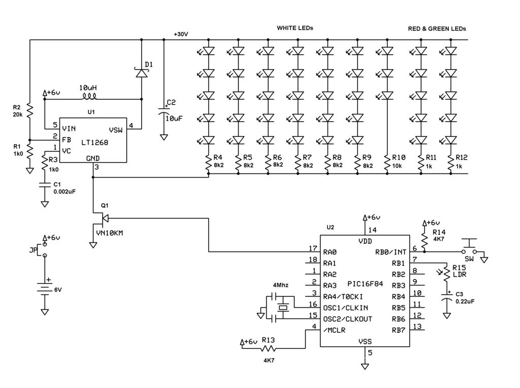
Make your own Boston Bomb
This is the circuit diagram. It is essentially a DC-DC converter, and a PIC 16F84 (or PIC 16F88) to drive it. SW1 is a test switch - push it to cause...
The described circuit involves a DC-DC converter, which is a...
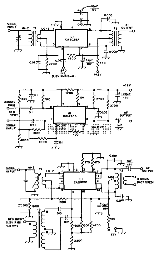
Ic Product Detectors
These product detectors utilize integrated circuit (IC) devices. They are capable of detecting single sideband (SSB) and continuous wave (CW) signals. The circuits are designed to operate effectively up to frequencies of 20 or 30 MHz. T3 in the schematic...