
Combination of common-source grounded emitter amplifier
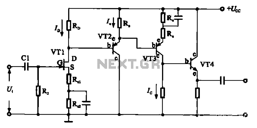
The described circuit integrates a common-source amplifier and a common emitter amplifier configuration to enhance the overall performance of the signal amplification process. The common-source amplifier, typically used in FET-based designs, provides high voltage gain, while the common emitter amplifier offers a balance of voltage and current gain with moderate input impedance.
In this configuration, the common emitter amplifier's input impedance is approximately 1.03 ohms, which presents a challenge for direct connections from the FET drive. To mitigate this issue, an emitter follower stage is introduced. The emitter follower, known for its high input impedance and low output impedance, serves as a buffer that allows for seamless interfacing between the FET and the common emitter amplifier. This configuration enhances the drive capability of the circuit, ensuring that the signal can be effectively transmitted without significant loss.
The load resistance (R_Tuen) is strategically connected to the common emitter amplifier to optimize the performance of the amplifier system. The inclusion of the emitter follower stage not only facilitates current gain but also stabilizes the output impedance, making it suitable for driving subsequent stages or loads that require a low impedance drive. This design exemplifies a robust approach to amplifier design, ensuring that both voltage and current gains are achieved while maintaining signal integrity and minimizing distortion.
Overall, this combination of amplifiers is ideal for applications requiring reliable amplification with efficient power handling, making it a valuable configuration in electronic circuit design. Combination of common-source grounded emitter amplifier A combination of common-source grounded pole radio amplifier. Common emitter amplifier input impedance in the range of l 03fl, it is difficult straight from the FET drive connected, however, if level through emitter follower, which as shown in FIG load R Tuen, connected to the common emitter amplifier the former, it is easy to drive, and as shown in FIG. The output stage circuit in front of the stage to join the emitter follower to get current gain, is an example of a typical low output impedance.
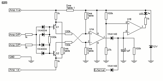
Related Circuits
At some stage, we will all find ourselves pushing hi-fi equipment just a little too hard, and if lucky, will just find that the sound has become "dirty". If this happens too often or is too severe, tweeters are...
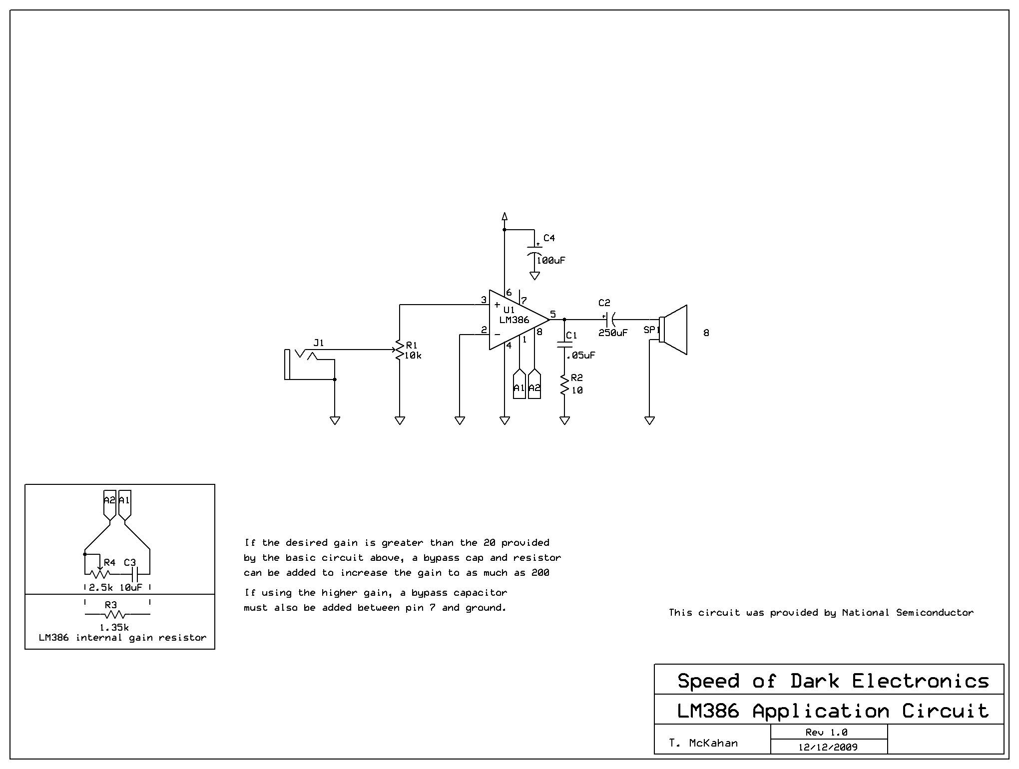
An LM386 Low Voltage Audio Amplifier was utilized for a project. The associated data sheet from National Semiconductor indicates that only five components are necessary for achieving a gain of 20, while seven components are required for a gain...
The converter depicted in Figure 1 utilizes a component from the PeakSwitch family (U1, a PKS606YN) to operate a 36 W motor, capable of handling startup and load transition peaks of up to 72 W. The motor speed can...
The amplifier circuit is well-suited for use in subwoofer speakers due to its robust performance. This circuit utilizes an integrated circuit (IC) based on the STK series. It can be employed in vehicles equipped with speakers or a subwoofer...
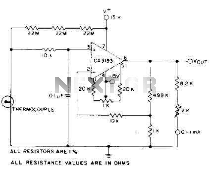
The circuit requires a 15-volt power supply and employs a precision operational amplifier, CA3193 BiMOS, to amplify the generated signal by more than 500 times. Three 22-megohm resistors are utilized to ensure a large-scale output in the event of...
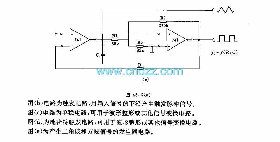
Figure a illustrates a multivibrator circuit capable of generating a square wave signal. Figure b depicts a flip-flop circuit that utilizes the falling edge of the input signal to produce a trigger pulse signal. Figure c represents a monostable...