Comparators
1. What is a Comparator?
1.1 What is a Comparator?
In the realm of electronics, a comparator is a crucial component that plays a significant role in a variety of applications, ranging from simple circuits to complex systems. At its core, a comparator is a device that compares two voltages or currents and outputs a digital signal indicating which is larger. This functionality is essential in facilitating decision-making processes within electronic systems, acting as a fundamental building block in analog to digital converters (ADCs), zero-crossing detectors, and various control applications.
Operational Overview
Comparators typically consist of two input terminals, labeled as inverting (−) and non-inverting (+), and a single output terminal. The output state of the comparator reflects the relationship between the two input voltages. When the non-inverting input voltage is greater than the inverting input voltage, the output is driven high, typically to the supply voltage. Conversely, when the inverting voltage exceeds the non-inverting voltage, the output is driven low, often to the ground. The transition between these states is not limited to fixed values; rather, it may depend on additional hysteresis introduced within the circuit to mitigate unwanted rapid switching due to noise, further stabilizing the operation.
Ideal and Non-Ideal Comparators
Ideal comparators have infinite gain and an infinite input impedance, which theoretically allows them to switch its output instantly with any differential voltage. In practice, real-world comparators exhibit limitations such as finite gain, finite response time, and input offset voltages. These nuances introduce challenges in circuit design; for instance, the inclusion of hysteresis—a mechanism where the threshold levels for switching are separated—can enhance noise immunity and prevent oscillations around the thresholds. Various configurations and topologies of comparators are designed to address these challenges, enabling their application in more demanding scenarios.
The connection between comparators and real-world applications cannot be overstated. They are integral to various electronic systems including:
- Threshold Detection: Comparators serve as threshold detectors in systems like smoke alarms and temperature control systems, where specific thresholds must be monitored.
- Analog-to-Digital Conversion: They play an essential role in ADCs where they compare an input signal against a reference voltage.
- Pulse Width Modulation: In control systems, comparators are used to create PWM signals, which are vital for efficient power management in motors and lights.
Conclusion
In summary, comparators serve as crucial components that facilitate decision-making in electronic circuits by comparing two signals. Understanding their operating principles, characteristics, and practical applications is vital for engineers and researchers alike, as they lay the foundation for advanced design and innovation in electronics. The knowledge of comparators empowers designers to create more efficient, reliable, and robust systems across a multitude of fields.
1.2 Comparator Basic Functionality
Comparators are fundamental building blocks in electronics, used extensively for signal processing. Their basic functionality is rooted in their ability to compare two input voltages and provide an output signal that indicates which input is higher. This section delves into the operational basics of comparators, their characteristics, and practical applications.
Understanding the Comparator Operation
At the core of a comparator is its operational principle, which involves comparing two input signals: an inverting input (denoted as Vin-) and a non-inverting input (Vin+). The output (Vout) of the comparator is determined by the following logical relationship:
The output state shifts based on the comparison of the two input voltages, typically switching between a high state (often referred to as Vhigh) and a low state (Vlow). This binary nature is what enables comparators to function effectively in digital circuits by providing a clear threshold level for signal processing.
Voltage Levels and Thresholds
In practical applications, comparators are often employed alongside reference voltage levels. The reference voltage helps in establishing a threshold, allowing the comparator to function as a decision-making device. The operation can be expressed as:
When Vin+ exceeds Vref, the output switches to Vhigh, indicating that the input signal is over the desired threshold. Conversely, if Vin+ is below Vref, the output is reduced to Vlow. This mechanism facilitates various applications, such as zero-crossing detection in signal processing and analog-to-digital conversion.
Real-World Applications
Comparators are found in numerous practical applications due to their ability to facilitate rapid voltage comparisons. Some common uses include:
- Overvoltage Protection: Utilized to monitor voltage levels and provide an alert or shutdown when exceeding safe thresholds.
- Signal Waveform Shaping: Applied in pulse width modulation (PWM) and analog to digital converters (ADCs) for generating square waves from sine waves.
- Hysteresis Circuits: Using feedback to stabilize comparisons, thus preventing rapid changes in output due to signal noise.
These applications highlight the versatility of comparators as essential components in electronic design, where precise voltage comparisons are crucial. After understanding their basic functionality, one can appreciate the underlying complexities and design considerations that engineers must account for when implementing comparator circuits.
1.3 Types of Comparators
Comparators are pivotal components in electronics, used for comparing two voltages or currents and producing a digital output indicating which is higher. Understanding the different types of comparators is essential for engineers, physicists, and researchers as they directly influence circuit design and application efficacy.Open-Loop Comparators
Open-loop comparators provide a simple and effective way to compare two analog signals without feedback. They function by amplifying the difference between their two input signals, typically using a high-gain operational amplifier in an open-loop configuration. The output swings to the supply rails, either high or low, depending on which input is greater. The primary advantage of open-loop comparators is their speed. However, they can be susceptible to noise, leading to instability and false triggering in certain conditions. Consequently, their practical applications are often seen in pulse-width modulation (PWM) circuits, detection of threshold levels in signal processing, and in zero-crossing detectors in waveform applications.Inverting and Non-Inverting Comparators
Within the paradigm of open-loop comparators, there are inverting and non-inverting comparators, distinguished by their input configurations. - Inverting Comparator: This configuration has one input tied to a reference voltage and the other to the input signal. The output is low when the input signal exceeds the reference voltage. Mathematically, if \( V_{\text{in}} > V_{\text{ref}} \), then \( V_{\text{out}} \) switches from high to low. This sets the comparator's output logic to '0' when the input is above a set threshold. - Non-Inverting Comparator: Conversely, this type outputs high when the non-inverting input exceeds the inverting input. The relationship can be mathematically expressed as \( V_{\text{out}} = V_{\text{CC}} \) when \( V_{\text{in}} > V_{\text{ref}} \). Artists of both configurations typically find usage in various applications, such as level comparators and voltage detectors.Hysteresis Comparators
To mitigate the issues of noise and instability seen in open-loop designs, hysteresis comparators were introduced. By integrating positive feedback into the comparator circuit, these devices create a band of voltage where the output remains steady despite fluctuations in the input signal. The hysteresis effect is characterized by two distinct threshold voltages: \( V_{\text{high}} \) and \( V_{\text{low}} \), ensuring that the output will only toggle when the input surpasses these levels. The stability provided by hysteresis makes these comparators ideal for applications requiring stable output amidst noise, such as in Schmitt triggers for square wave generation or in zero-cross detectors.Window Comparators
Window comparators are designed to output a signal based on whether the input voltage falls within a predefined range or 'window'. This is achieved by using two comparators, one configured to activate when the input crosses a lower threshold and another for the upper threshold. The output is typically high only when the input voltage lies between these two thresholds. These devices find practical use in applications involving over-voltage protection, battery voltage monitoring, and other systems requiring precise control over the voltage levels within a given range.Analog Comparators
Analog comparators, distinct from their digital counterparts, produce an output that is a function of the paths and amplitudes within the input signal ranges. They can be designed to generate a proportional output based on the difference between two input signals, making them suitable for applications such as analog-to-digital converters (ADCs) where fine resolution is critical. While their design is more complex than that of standard comparators, they offer superior performance in applications necessitating high precision in measurement and output fidelity.Real-World Applications
The diversity of comparator types offers a spectrum of applications in real-world scenarios. Open-loop comparators are widely employed in timing circuits, while hysteresis comparators serve as fundamental blocks in switch-mode power supplies. Moreover, window comparators play crucial roles in sensor applications, aiding in the development of smart systems in industrial automation and automotive electronics. Understanding the nuances of each type enables advanced professionals in the field to select the right comparator for their specific needs, ensuring optimal functionality and robustness in electronic designs. In conclusion, the advancement and selection of comparators necessitate a closer examination of their operational principles, distinct types, and the varying applications they serve, highlighting their critical role in modern electronics.2. Open-Loop Comparators
2.1 Open-Loop Comparators
Open-loop comparators are fundamental components in the field of electronics, particularly in analog signal processing. They are designed to compare two input voltage levels, producing a binary output based on which input is greater. This section explores the operational principles, design considerations, and practical applications of open-loop comparators.
Basic Principles of Operation
At its core, the open-loop comparator consists of an operational amplifier (op-amp) with no feedback loop. When two input voltages, \(V_+ \) and \(V_- \), are applied to the op-amp, it amplifies the difference between these inputs. The output voltage, \(V_{out} \), is determined by the equation:
Where \(A\) represents the open-loop gain of the op-amp, typically exceeding 100,000 for many operational amplifiers. This high gain results in an output that swings nearly to the positive or negative supply voltage levels based on the input comparison.
Threshold Levels and Hysteresis
In practical applications, it is important to consider threshold levels for the inputs. For a comparator to switch states, the input voltage needs to surpass these defined thresholds. The output will flip states when \(V_+ > V_- \) transitions from a lower voltage to a higher voltage. This can lead to unwanted oscillations or instability, especially in noisy environments. To combat this, hysteresis can be introduced into the design, shifting the threshold levels for turn-on and turn-off, thus enhancing stability.
The hysteresis can be implemented using positive feedback, which adds a small portion of the output back into the non-inverting input. The modified input condition can be represented as:
Where \(V_{th+} \) and \(V_{th-} \) denote the upper and lower threshold voltages, respectively, and \(V_{hyst} \) represents the hysteresis voltage magnitude.
Applications in Circuit Design
Open-loop comparators find use in a myriad of applications due to their rapid response times and binary output behavior. Some common applications include:
- Zero-Crossing Detectors: Used in phase-locked loops and sinusoidal signal processing to detect when a signal crosses the zero voltage point.
- Voltage Level Detectors: Monitoring voltage levels for triggering devices such as alarms or indicators in power management systems.
- Switching Applications: Used in control systems for turning devices on/off based on varying input conditions, such as thermostats.
Conclusion
Open-loop comparators are simple yet powerful devices that contribute critically to various electronic systems. While they operate based on straightforward principles, considerations such as voltage thresholds and stability become significant in real-world scenarios. Further exploration into feedback methods and advanced algorithms can optimize their performance, adapting to more complex applications in modern electronics.
2.2 Closed-Loop Comparators
Closed-loop comparators are an essential category of comparators that incorporate feedback mechanisms, enabling them to maintain excellent accuracy and stability over a wide range of input conditions. Unlike open-loop comparators, which simply compare two voltages and output a high or low signal based on the comparison, closed-loop comparators utilize feedback to modulate their output, adjusting performance characteristics dynamically.
At a fundamental level, closed-loop comparators consist of an operational amplifier operating in a negative feedback configuration. This feedback modifies the gain and response of the comparator, significantly improving linearity and precision. The output of the comparator is influenced not only by the difference between the input voltages (the non-inverting input and the inverting input) but also by the feedback voltage derived from the output. The core operation can be represented accurately by the equation:
Here, \( A \) represents the open-loop gain of the operational amplifier, while \( V_{+} \) and \( V_{-} \) are the voltages at the non-inverting and inverting inputs, respectively. Unlike in an open-loop configuration where \( V_{out} \) is saturated either at the positive or negative supply voltage, closed-loop operation allows for more versatile output conditions based on the application demands.
Design Considerations
When designing a closed-loop comparator, several key aspects involved include:
- Hysteresis: Introducing hysteresis can prevent the output from rapidly toggling due to small fluctuations or noise in the input signal, which is crucial in applications like signal conditioning.
- Bandwidth: The frequency response must be sufficient for the intended application. Feedback can affect the bandwidth and settling time of the comparison.
- Power Supply: Consideration of the supply voltage is important, especially in battery-operated devices where efficiency and power constraints are significant.
These aspects emphasize the practical relevance of closed-loop comparators in real-world applications. For instance, they are extensively used in precision voltage level detection, zero-crossing detection, and analog-to-digital conversion applications. By offering a more stable and accurate response to voltage comparisons, they springboard advancements in fields ranging from automated manufacturing to consumer electronics.
Applications in Modern Electronics
Closed-loop comparators find usage in circuits that operate under varying conditions requiring robust performance. For example:
- Pulse Width Modulation (PWM): In motor control applications, closed-loop comparators modulate the duty cycle of PWM signals based on feedback from motor performance, improving efficiency and response time.
- Threshold Detectors: In sensor applications, closed-loop comparators can determine when a signal crosses a threshold, enabling instant responses to changes in environmental conditions.
This heightened responsiveness linked with effective feedback mechanisms demonstrates why closed-loop comparators are favored in analytical instrumentation, robotics, and other critical systems where precision timing and measurement are paramount.
To summarize, closed-loop comparators leverage operational amplifiers in feedback configurations to enhance stability, accuracy, and responsiveness in voltage comparison applications. Their design involves considering various parameters such as hysteresis, bandwidth, and power supply, underscoring their versatility and utility across numerous domains.
2.3 Voltage Level Comparators
Voltage level comparators are fundamental electronic devices used to compare two voltage levels and output a corresponding binary signal. This capability is essential in numerous applications, from simple voltage measuring circuits to advanced digital logic systems. By utilizing a comparator, engineers and physicists can create systems that are faster and more efficient, marking the significance of this component in both theoretical and practical realms.
At their core, voltage level comparators operate on a simple yet powerful principle: they measure the difference between a reference voltage and the voltage signal of interest. This comparison can be visualized in terms of two input terminals, usually referred to as the inverting (-) and non-inverting (+) inputs. When the voltage at the non-inverting input exceeds that at the inverting input, the output transitions to a high state; conversely, if the inverting input has a higher voltage, the output switches to a low state.
Operational Amplifier as a Comparator
A common realization of a voltage level comparator is through the use of operational amplifiers (op-amps). In this configuration, the op-amp operates in an open-loop mode, which means no feedback is provided to control the gain. This results in the output saturating to the supply voltage levels when the inputs differ. Let's derive the output equation for an ideal comparator:
Given an op-amp with an open-loop gain A, the output voltage V_out relates to the differential input voltage V_d as:
Where:
In the case of voltage level comparison, the output will saturate to either the positive or negative supply voltage depending on the condition of the input voltages:
- If \( V_{+} > V_{-} \): \( V_{out} \approx V_{CC} \)
- If \( V_{+} < V_{-} \): \( V_{out} \approx V_{EE} \)
This simple but effective mechanism underpins various applications—from zero-crossing detectors in audio devices to voltage level detection in digital circuits.
Real-World Applications
Voltage level comparators have numerous applications across different fields, significantly impacting both industrial and consumer electronics:
- Voltage Level Shifters: In mixed-signal systems, comparators ensure compatibility between different voltage levels, preventing damage and ensuring reliable operation.
- Window comparators: By employing multiple reference voltages, these comparators can create ranges within which an input voltage can be accurately monitored. This is crucial in protection circuits and monitoring systems.
- Analog-to-Digital Conversion: Comparators serve as integral components in ADCs, assisting in the quantization of continuous signals into discrete levels.
Moreover, the analog behavior of comparators importantly translates into the digital domain, paving the way for more complex digital systems that leverage threshold detection mechanisms in areas such as signal processing and control systems.
Considerations for Practical Applications
When selecting a voltage level comparator for a specific application, several critical factors must be considered:
- Response Time: The switching speed is crucial, especially in high-frequency applications.
- Input Offset Voltage: This characteristic affects accuracy; lower offset voltage is preferable in precision applications.
- Power Supply Requirements: Ensure that the comparator's supply voltage meets the system requirements without compromising performance.
Overall, voltage level comparators are vital for a wide range of circuits, serving as a backbone for decision-making processes that rely on voltage comparisons. Their integration into new technologies continues to enhance the functionality and reliability of modern electronic devices.
3. Input Characteristics
3.1 Input Characteristics
The input characteristics of comparators play a crucial role in determining their performance and applicability in various electronic circuits. Comparators are devices that compare two voltages or currents and output a digital signal indicating which is larger. An in-depth understanding of their input characteristics is essential for engineers and researchers aiming to apply these components in real-world situations.
Voltage and Current Inputs
In most comparator applications, input signals are either voltage or current. The voltage input is the more common form, where the comparator assesses two input voltages, V+ (non-inverting input) and V− (inverting input). The output state of the comparator is determined by whether V+ is greater than or less than V−.
Let's denote the comparator's output as Vout. The relationship is defined as follows:
Here, Vsat is the saturation voltage of the comparator, a parameter dependent on the specific characteristics of the device being used. Understanding these parameters becomes critical when ensuring that the operating conditions remain within specified limits—thus maintaining precise operation.
Input Impedance
Input impedance is another key characteristic that impacts the performance of comparators. High input impedance is desirable as it minimizes the loading effect on the input signals. This characteristic is particularly important in applications like sensor interfacing where the input voltage signals can be very weak.
The input impedance of comparators is typically in the range of megaohms (MΩ). However, this value can be influenced by the internal circuitry of the comparator, such as the inclusion of any biasing resistors. A general model may assume:
Where Rin is the input resistance of the comparator and Rsource is the resistance of the signal source. This inequality ensures that the input signal is not significantly altered by the comparator's characteristics.
Common Mode Range and Input Offset Voltage
Additionally, the common mode range is crucial as it defines the limits within which both V+ and V− can operate effectively without degrading performance. It's important to select comparators whose common mode range encompasses the expected voltages applied to the inputs in a given application.
Furthermore, the input offset voltage, often represented as VOS, is the differential input voltage required to make the output zero. A lower input offset voltage is desirable for high-precision applications, such as analog-to-digital converters, where accuracy is paramount:
Thermal and Noise Sensitivities
Thermal effects and input noise can also affect the performance of comparators. Temperature variations can introduce drift, which impacts the reliability of the output under varying operating conditions. Further, noise can cause false triggering, especially in high-speed applications. Designing appropriate filtering on the inputs can mitigate some of these issues and improve the overall stability and accuracy of the comparator.
With a thorough understanding of these input characteristics, engineers can better design comparator circuits that are robust, reliable, and suitable for demanding applications.
3.2 Output Characteristics
In exploring the functionality of comparators, we must next delve into their output characteristics, which play a critical role in how these devices are employed in practical applications. The output characteristics of a comparator primarily involve how the output voltage responds to the input signals—essentially defining the behavior of the comparator as it compares two voltage levels. The comparator's output can typically adopt one of two modes based on the conditions of its inputs: the standard output states (high and low) exhibit digital behavior, while some comparators offer an analog output, providing a continuous range between extremes. Understanding these scenarios is vital for engineers and researchers who seek to implement comparators in real-world systems such as analog-to-digital converters (ADCs), zero-crossing detectors, or even more complex logic systems.Output States
To formally characterize the output, we can discuss the two primary states: 1. High State: When the non-inverting input (V+) exceeds the inverting input (V-), the comparator’s output tends to its upper limit, commonly near the power supply voltage (often denoted as Vcc). In this state, the output can be thought of as a digital "1". 2. Low State: Conversely, when V+ is less than V-, the output drops to approximately the lower supply voltage or ground (Vss), effectively representing a digital "0". The transition between these states can be abrupt, and this behavior can be modeled mathematically using the characteristics of the comparator circuit, focusing on the gain and speed of response.Mathematical Representation
To derive the essential equations governing the output transition, we can assume an ideal comparator with infinite open-loop gain (A). When V+ = V- at threshold voltage (Vt), the equation for gain can be represented as: $$ V_{out} = A \times (V_{+} - V_{-}) \quad \text{for an ideal comparator} $$ With infinite gain, any minute difference between V+ and V- will drive the output swiftly to either Vcc or Vss. Practically, if A is large, we consider regions where: - For V+ > V-, $$V_{out} \approx V_{cc}$$ - For V+ < V-, $$V_{out} \approx V_{ss}$$ This characteristic defines the hysteresis of the comparator, which describes how input variations affect the output state. Implementing a feedback mechanism can modify the threshold voltages and minimize noise-induced transitions, enhancing the stability of the output signal.Real-World Applications
The sharp transitioning nature of the output signal reflects an essential purpose in various applications: - Voltage Level Detection: Comparators can serve as level detectors, suitable for ensuring system voltage levels remain stable, which is critical in systems like power management. - Window Comparators: By configuring two comparators, one can establish a window comparator function to monitor voltage against both upper and lower thresholds, allowing for effective monitoring of battery levels in portable devices. - Signal Conditioning: In signal processing applications, comparators help ensure clean transitions, filtering out noise from analog signals before they are digitized. Armed with this knowledge of output characteristics, practitioners can choose the right comparator configuration and set it up for optimal performance in their designs. With technology continuously evolving, further innovations will likely refine these characteristics to suit increasingly specific requirements in targeted applications.3.3 Response Time and Hysteresis
In the realm of comparators, two critical parameters that greatly influence their performance are response time and hysteresis. Understanding these aspects can help engineers design more reliable circuits that meet the specific needs of applications in various domains, such as control systems, signal processing, and data acquisition.Response Time of Comparators
The response time of a comparator refers to the speed at which the comparator can switch its output from one state to another in response to a change in the input signal. It is defined as the time it takes for the output voltage to reach a specified percentage of its final value after a step change at the input. The response time is crucial in high-speed applications because it directly affects the overall system performance. To illustrate this concept, consider a comparator that receives a step input at time \( t = 0 \). The output response can be approximated by a first-order transfer function:- Input Signal Slew Rate: A slower input signal may result in a longer response time.
- Circuit Load: Heavy loads can delay the response due to increased capacitance.
- Temperature Variations: Changes in temperature can affect the component characteristics, altering the response.
Understanding Hysteresis
Hysteresis in comparators is an essential feature that helps prevent false triggering due to noise in the input signal. In simple terms, hysteresis refers to the difference in input voltage levels at which the output changes states; one level for rising input and a different one for falling input. This characteristic is vital for ensuring stable operation in noisy environments. When a comparator is subject to thresholds defined by hysteresis, the circuit exhibits a characteristic transfer curve resembling a loop: Transfer Characteristics with Hysteresis Diagram [Diagram depicting the relationship between input voltage and output states, illustrating the upper threshold for switching high and the lower threshold for switching low]. Mathematically, the upper and lower threshold voltages can be defined as:4. Zero-Crossing Detectors
4.1 Zero-Crossing Detectors
Zero-crossing detectors are a specific type of comparator circuit that play a crucial role in converting analog signals into digital ones by identifying when a signal crosses the zero-voltage level. This is particularly important in applications like phase-locked loops, phase detection, and signal conditioning where precise timing and synchronization are essential.
At their core, zero-crossing detectors make use of the properties of voltage comparators, which compare two input voltages and output a high or low state based on their relative magnitudes. In the case of a zero-crossing detector, one of these inputs is typically grounded (0V), and the other is the input signal whose zero crossings we wish to detect.
Operating Principle
The fundamental operation of a zero-crossing detector can be understood through its response to an alternating current (AC) signal. When an AC signal oscillates, it crosses the zero-voltage mark twice during each cycle: once when it transitions from positive to negative, and again when moving from negative to positive. The detector, thus, must discern these transitions effectively.
A simple configuration can be described using an operational amplifier (op-amp) functioned as a comparator. The op-amp compares the voltage of the incoming signal to that of a reference voltage at 0V. When the input signal is above 0V, the output state of the op-amp is high (typically at the positive supply voltage). Conversely, when the input signal is below 0V, the output switches to low (often near ground level). This switching behavior provides digital pulses indicating the zero crossings of the input AC signal.
Mathematical Representation
To describe the operation rigorously, consider the input voltage \( V_{in}(t) \) that can be represented as a sinusoidal wave:
Where \( V_m \) is the maximum amplitude and \( \omega \) is the angular frequency. The zero-crossing points occur at:
For each complete cycle of the sine wave, there are two points (n = even and n = odd) where \( t_{zero} \) indicates transitions through zero, resulting in a shift in the output of the comparator.
Practical Circuit Design
A popular implementation of a zero-crossing detector is shown in the figure below. The circuit consists of an op-amp with a non-inverting input connected to the AC signal and an inverting input grounded. A feedback resistor may be included to adjust the gain if necessary, ensuring rapid switching to minimize delays leading to erroneous timing results.
This design can be used in various applications, including:
- Phase-Locked Loops (PLLs): Used in frequency synthesis and demodulation.
- Signal Conditioning: Provides a clean digital representation of noisy sinusoidal inputs.
- Timer Circuits: The precise zero-crossing signals can be used to trigger timing events in digital systems.
However, it’s crucial to note that zero-crossing detection can be influenced by noise. If the input signal exhibits significant noise at the zero-crossing point, false triggering may occur. Implementing hysteresis through positive feedback can mitigate this issue, creating a more robust output against noise interference.
In summary, zero-crossing detectors are critical components in modern electronic systems, providing the necessary interface between analog and digital worlds, enabling precise control and measurement in various applications.
4.2 Analog-to-Digital Converters
Analog-to-Digital Converters (ADCs) are pivotal components in bridging the gap between the real world and the digital realm. They transduce continuous analog signals, which can take any value within a range, into discrete digital numbers that can be processed by digital systems. At the heart of an ADC is a comparator, which plays a critical role in determining the binary level corresponding to the input voltage.
Understanding the Basics of ADCs
In essence, the ADC samples the input analog signal at a certain sampling rate and quantizes these samples into a finite number of levels. This process of quantization directly relates to the resolution of the ADC, typically described in bits. A higher resolution allows the ADC to represent the analog input with finer granularity. For example, an 8-bit ADC can represent 256 discrete levels, whereas a 12-bit ADC can distinguish 4096 levels, thereby providing a more precise representation of the input signal.
The operation of the ADC generally involves two significant stages: sampling and quantization. In the sampling phase, a sample-and-hold circuit captures values of the analog signal at discrete intervals, while the quantization phase converts each sampled voltage to the nearest available digital level. The output of this conversion process can be mathematically represented as:
Here, \( D \) represents the digital output, \( V_{in} \) is the input voltage, \( V_{min} \) is the minimum voltage of the ADC, and \( V_{step} \) is the voltage corresponding to one quantization level, calculated as \( \frac{V_{max} - V_{min}}{2^N} \), where \( N \) is the number of bits in the ADC.
Types of ADCs
There are several types of ADC architectures, each with its own unique operational principles and applications. Some of the most common types include:
- Successive Approximation Register (SAR) ADC: Widely used due to their balance of speed and resolution, SAR ADCs utilize a binary search algorithm to converge on the digital value.
- Delta-Sigma ADC: Known for high-resolution applications, these converters oversample and use digital filters to improve noise performance.
- Flash ADC: Offering very high speed, Flash ADCs use a voltage ladder and a series of comparators to produce the digital output in a single step, suitable for applications requiring rapid conversion.
Comparator Role in ADCs
In ADCs, the comparator's function is to compare the input voltage with reference voltages during the quantization stage. The choice of reference voltages and the speed of the comparator heavily influences the overall performance, particularly in SAR and Flash ADC architectures. Optimal design of comparators, including the use of hysteresis to minimize the effects of noise, is critical in ensuring accurate and stable conversions.
Real-World Applications of ADCs
ADCs find applications in various fields, including:
- Signal Processing: Converting analog signals from sensors into digital signals for further processing in applications like audio recording and telecommunications.
- Medical Electronics: In devices such as ECG machines, ADCs digitize physiological signals for monitoring and analysis.
- Industrial Automation: Utilized in data acquisition systems to monitor and control processes, ensuring system efficiency and reliability.
As we continue to integrate more analog components into the digital world, the importance of ADCs and their underlying comparators remains paramount for leveraging the power of data in various applications. Understanding these systems not only aids in the design of better circuits but also equips engineers and researchers with the tools to innovate in a rapidly evolving technological landscape.
4.3 Threshold Detectors
Threshold detectors are an important class of comparators that serve as a fundamental building block in various electronic components and systems. These devices are designed to trigger state changes when an input signal crosses a predetermined threshold value. Understanding their operation and applications can provide insights into the design of sensors, signal processing systems, and control mechanisms.
Operating Principle
The core functioning of a threshold detector revolves around comparing an input voltage to a reference voltage. When the input voltage exceeds this reference threshold, the output state changes, typically switching from low to high (or vice versa). This simple binary decision-making capability allows threshold detectors to be utilized in a wide range of applications, where detecting specific signal levels is crucial.
Types of Threshold Detectors
Threshold detectors can be broadly classified into two categories: positive-going and negative-going detectors.
- Positive-going threshold detectors activate when the input voltage surpasses the reference voltage, signaling a 'high' state.
- Negative-going threshold detectors activate when the input voltage falls below the predetermined reference value, signaling a 'low' state.
This duality allows designers to select the appropriate configuration based on the requirements of their specific application.
Mathematical Representation
To understand the mathematical underpinnings of threshold detectors, consider a basic model:
Let \( V_{in} \) be the input voltage, and \( V_{th} \) be the threshold voltage. The output \( V_{out} \) can be defined as:
In this equation, \( V_{high} \) represents the output voltage when the input exceeds the threshold, while \( V_{low} \) represents the output when the input is below the threshold. The transition between these states can be sharp, particularly in well-designed detectors, which ensures fast response times suitable for many real-time applications.
Practical Applications
Threshold detectors find utility in numerous domains. Notably, they are employed in:
- Signal Conditioning: Used in sensors to filter noise and ensure that only significant signals are processed, thereby enhancing the reliability of systems.
- Level Shifting: In power management systems, they help in detecting over-voltage or under-voltage conditions, safeguarding circuits from damage.
- Data Converters: In Analog-to-Digital Converters (ADCs), threshold detectors play a crucial role in sampling and converting signals efficiently.
- Comparators in Oscillators: Used to maintain a specific frequency by triggering state changes based on threshold levels.
These applications illustrate the versatility and importance of threshold detectors in real-world electronic systems. Their simple yet effective operation makes them indispensable in both industrial and consumer electronics.
Conclusion
In summary, threshold detectors serve as vital tools in electronic engineering, enabling the detection and processing of signals based on defined voltage levels. Their design can significantly influence the performance and reliability of various applications, making a deep understanding of their mechanics essential for engineers and researchers alike.
As technologies evolve, the integration of threshold detectors will only grow, responding to the increasing complexity of electronic systems.
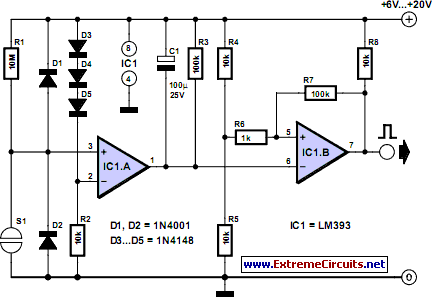
5. LM393 Comparators
5.1 LM393 Comparators
Introduction to LM393 Comparators
The LM393 is a widely used dual comparator integrated circuit known for its ability to provide comparative analysis of two voltage levels. With applications ranging from signal detection to zero-crossing detection in audio and control systems, it serves as a critical building block in various electronic devices. The LM393 can operate effectively in the linear region, enabling a broad range of functionalities in real-world applications.
Fundamental Operation of the LM393
The LM393 comprises two independent voltage comparators; each can compare two input voltages, producing a corresponding output voltage. The output is a digital signal indicating whether the non-inverting input (+) is greater than or less than the inverting input (−). This functionality can easily be visualized as a binary decision-making process.
When analyzing the behavior of the LM393, a key characteristic is the ability to operate with a single supply voltage, allowing it to function effectively in battery-operated devices. Its input voltage range can span from the negative supply (ground) to just below the positive supply voltage, typically 32V, making it versatile across different applications.
Mathematical Representation
The operation of the LM393 can be mathematically described by the following conditions:
Here, \(V_{CC}\) is the supply voltage, \(V_+\) is the voltage at the non-inverting input, and \(V_-\) is the voltage at the inverting input. The output of the comparator swings to \(V_{CC}\) when the condition \(V_+ > V_-\) is satisfied, and it goes to 0 otherwise, reflecting the binary nature of its operation.
Practical Applications of LM393 Comparators
LM393 comparators find extensive use in a variety of applications, including:
- Voltage Level Monitoring: In systems where specific voltages must be monitored and controlled, such as battery management systems, LM393 can trigger alerts or actions based on voltage thresholds.
- Analog to Digital Conversion: It serves as an essential component in analog-to-digital converter circuits, helping to delineate voltage levels for processing.
- Zero-Crossing Detection: In audio applications, the device can be employed to detect when an audio signal crosses the zero-volt level, facilitating noise reduction and signal processing.
- Temperature Sensing: Coupled with thermocouples, LM393 comparators can be used to create temperature-sensing circuits by comparing output voltage with a predetermined threshold.
Conclusion
The LM393 comparator stands out due to its efficiency, versatility, and reliability in various electronic applications. Understanding its operational principles and practical implementations can empower engineers and researchers to design sophisticated circuits tailored to specific needs, ultimately advancing the functionality of modern electronic systems.
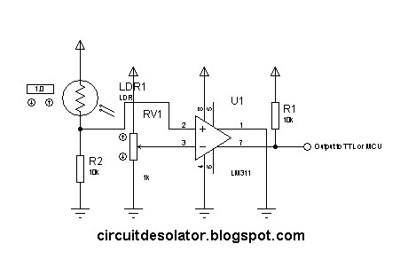
5.2 LM339 Comparators
In the realm of electronic circuit design, comparators play a critical role. They are essential for comparing two input voltages and producing a binary output, indicating which of the two is higher. Among the various comparator ICs available, the LM339 stands out due to its versatility and reliability in multiple applications. The LM339 is a quad comparator, meaning it consists of four independent comparators within a single package. This feature significantly enhances design efficiency, as it reduces the number of components required. The device operates in a voltage range of 2V to 36V, making it applicable in various low- to mid-voltage systems. Its outputs can be configured for open collector applications, allowing for simple interfacing with other digital logic families and enabling wired-AND logic configurations. One of the defining characteristics of the LM339 is its ability to operate with low input currents, making it suitable for battery-operated devices and applications that demand low power consumption. This is particularly advantageous in sensor applications where power efficiency is paramount. The LM339 can also handle input voltages that swing below ground, which allows for comparison in differential signal scenarios, broadening its utility. To understand how the LM339 operates in a circuit, consider the fundamental topology of a comparator. When the non-inverting input voltage exceeds that of the inverting input, the output transitions to a low state (ground potential) if the output is set to a pull-up resistor. Conversely, when the inverting input voltage is greater, the output returns to a high impedance state. This behavior can be mathematically described as follows: Let \( V_{+} \) be the voltage at the non-inverting input and \( V_{-} \) be the voltage at the inverting input. The output can be defined as:Key Features of LM339
- Quad Comparator: Four comparators in one package reduce circuit complexity.
- Wide Supply Voltage Range: Operates from 2V to 36V.
- Low Input Current: Ideal for low-power and battery-operated applications.
- Open Collector Output: Facilitates various logic configurations, enabling flexibility in design.
- Input Voltage Rail-to-Rail: Can handle inputs below ground, enhancing versatility.
5.3 Comparators in Integrated Circuits
Comparators serve a pivotal role in the realm of integrated circuits (ICs), acting as fundamental building blocks for various applications, from simple signal processing to complex analog-to-digital conversion schemes. By their very nature, comparators are devices designed to compare two input voltages and output a digital signal, indicating which input is larger. Understanding their operation within integrated circuits not only unveils the principles of analog signal processing but also demonstrates their indispensable utility in modern electronics.
Historically, the evolution of comparators correlates with the advancements in semiconductor technology. Early implementations were realized with discrete components, but as integration technology progressed—especially with the advent of CMOS technology—comparators evolved, leading to the compact and efficient designs we see in contemporary integrated circuits. Figures such as the LM339 and the LM393 highlight this transition, as they represent low-power, versatile comparators widely used across various applications.
Working Principle of Comparators
At the heart of a comparator lies a differential amplifier configuration, where two input voltages are fed into the non-inverting (+) and inverting (−) terminals. The output of the comparator depends on the voltage levels applied at these terminals:
- When the voltage at the non-inverting terminal is higher than that at the inverting terminal, the output swings high, approaching the positive supply voltage.
- Conversely, when the inverting terminal's voltage exceeds that of the non-inverting terminal, the output drops to the negative saturation level (typically ground in single-supply configurations).
This transition occurs rapidly, enabling comparators to serve as effective decision-making elements in high-speed applications.
Where: Vout is the output voltage, V+ is the positive supply voltage, V- is the negative saturation voltage (often ground), Vin+ is the voltage at the non-inverting terminal, and Vin- is the voltage at the inverting terminal.
Characteristics Relevant to Integrated Circuits
In integrated circuits, several key characteristics of comparators are especially important:
- Input Offset Voltage: This is the differential DC voltage required between the input terminals to bring the output to zero. Lower offset voltage is critical for precision applications.
- Propagation Delay: The time it takes for the output to reflect a change in the input signal. Minimizing this delay is crucial for high-speed operations.
- Common Mode Range: The range of input voltage levels that do not affect the performance of the comparator. A wider range allows greater design flexibility.
- Saturation Voltage: This refers to the output voltage level when the comparator is in saturation. Lower saturation voltages facilitate better signal integrity.
These characteristics guide the design and selection processes of comparators in integrated circuits—affecting factors such as power consumption, speed, and accuracy.
Applications of Comparators in Integrated Circuits
The impact of comparators is vast, with applications spanning multiple domains:
- Zero-Crossing Detectors: Used in phase-locked loops or AC signal processing to detect the points where the signal crosses zero voltage.
- Voltage Level Shifters: Comparators can shift digital signals from one voltage level to another, facilitating communication between different logic levels.
- Analog-to-Digital Converters (ADCs): Comparators form the basis of successive approximation ADCs, comparing input signals to reference levels during the conversion process.
- Schmitt Trigger Circuits: Comparators with hysteresis characteristics are used to convert noisy signals into clean digital transitions.
The real-world applications of comparators extend into automotive systems, industrial control, communication devices, and consumer electronics, demonstrating their critical role in modern technology.
Examining the advantages and performance metrics of comparators allows engineers and researchers to optimize their designs, ensuring effective signal processing and interfacing in today's rapidly advancing electronic landscape.
6. Noise and Interference
6.1 Noise and Interference
In the realm of electronic signal processing, comparators play a vital role in distinguishing between two voltage levels. However, the performance of these devices can be significantly affected by noise and interference. Understanding how these factors influence comparator circuits is crucial for engineers and researchers working on precision applications. Noise, in a broad sense, refers to any unwanted electrical fluctuations that obscure the true signal. In the context of comparators, noise can introduce false triggering, leading to erroneous outputs. This undesirable phenomenon can be particularly problematic in systems requiring high accuracy, such as analog-to-digital converters (ADCs) or in fast-switching applications where precision timing is essential. To analyze noise, we can classify it into two primary categories: thermal noise and shot noise. Thermal noise arises from the random motion of electrons in a resistive material and can be modeled by- Filtering: Low-pass filters can effectively reduce high-frequency noise while preserving the integrity of the desired signal.
- Hysteresis: Implementing hysteresis in comparator designs creates a margin for error, which offers resistance to noise-induced fluctuations.
- Shielding and Grounding: Properly shielding sensitive circuits and establishing robust grounding can help reduce susceptibility to external interference.
6.2 Comparator Unstable Output
In the realm of comparators, the unstable output phenomenon refers to scenarios where the output state of the comparator oscillates uncontrollably rather than settling into a distinct high or low state. This behavior is frequently observed in applications involving noise, interference, or rapid changes in input signals. Understanding the mechanisms behind unstable outputs is essential for engineers and researchers to develop reliable comparator circuits that perform predictably in real-world environments.
Mechanisms of Unstable Output
Unstable outputs can arise from several factors inherent in the comparator's operation:
- Hysteresis: Comparators often lack hysteresis, making them sensitive to small fluctuations or noise on the input signal. When the input is near the threshold voltage, even minor variations lead to toggling of the output.
- Input Impedance: High-impedance environments can exacerbate noise susceptibility, making the comparator react to insignificant signal perturbations.
- Supply Voltage Instability: Variations in the supply voltage can shift the reference thresholds, altering the comparator's decision-making process.
This unstable output behavior may not present immediate challenges in some applications, but it can lead to significant problems in precision work, data acquisition systems, and digital signal processing where reliability is paramount.
Case Study: Schmitt Trigger as a Solution
The Schmitt trigger is an effective solution to mitigate unstable output by introducing controlled hysteresis. By adding positive feedback, the Schmitt trigger creates distinct transition voltage levels for switching between the high and low states. This means that the input must cross a certain threshold to switch output states, thereby reducing sensitivity to noise. In practical circuit design, a basic Schmitt trigger can be constructed using a standard operational amplifier (op-amp) configured with feedback resistors to set the upper and lower thresholds. This configuration stabilizes the output, providing a robust response to varying input signals.
In this equation, \( V_{th\_high} \) and \( V_{th\_low} \) represent the upper and lower threshold voltages, respectively, establishing the framework for the Schmitt trigger's behaviour under varying \( V_{in} \).
Practical Applications
Understanding and addressing unstable outputs is crucial in numerous applications:
- Signal Conditioning: In analog signal processing, ensuring stability in comparator outputs is essential for producing clear and accurate signals.
- Embedded Systems: Microcontrollers often utilize comparators for various functions; unstable outputs can lead to unreliable performance in safety-critical applications.
- Data Acquisition Systems: In measurement systems, noise can lead to erroneous data interpretation; thus, stable comparator outputs are critical for data integrity.
As engineers continue to push the boundaries of technology, managing unstable comparator outputs will remain an essential skill set, underpinning countless electronic systems' reliability and performance.
6.3 Power Supply Considerations
Understanding Power Supply Requirements
When designing circuits involving comparators, the choice and management of the power supply are crucial factors that can affect performance, stability, and reliability. Comparators are often used in various applications, such as analog signal processing, threshold detection, and embedded systems. Thus, the quality of the power supply directly influences the comparator's accuracy and response time.
Voltage Levels and Supply Configuration
Most comparators operate within specific voltage ranges, commonly referred to as the positive supply voltage (V+/VDD) and negative supply voltage (V-). For single-supply applications, a ground reference is typically paired with a positive voltage. In contrast, dual-supply configurations utilize both positive and negative voltages.
For example, an open-loop comparator with a single supply of +5V could have an operational range of approximately 0 to +5V. The selected power supply must align with the output swing of the comparator. Most modern comparators can achieve rail-to-rail output, meaning their output can swing to very near the power supply levels.
Noise and Stability Considerations
Power supply noise can introduce unwanted variations in the output of comparators, leading to false triggering and erroneous behavior. Decoupling capacitors are indispensable components in the design, used to filter out high-frequency noise from the power supply. Strategically placing these capacitors close to the power pins of the comparator helps maintain stability.
To quantify the impact of voltage fluctuations, let's consider the power supply rejection ratio (PSRR). PSRR indicates how well a device can reject variations in power supply voltage. This characteristic is critical when designing high-precision analog circuits.
Here, $$\Delta V_{out}$$ represents the change in output voltage due to a change in supply voltage $$\Delta V_{supply}$$. A higher PSRR value signifies better performance against supply variations, which is especially important in comparator applications.
Power Supply Sequencing
In circuits involving multiple components, proper power supply sequencing becomes necessary to prevent latch-up conditions and ensure reliable startup behavior. This process involves powering up various components in a predefined order, preventing high current from prematurely activating sensitive devices. Implementing a controlled ramp-up of power can mitigate these risks.
Temperature Effects on Power Supply Performance
Finally, it's worth noting that temperature variations can affect the performance of power supply components such as voltage regulators and capacitors. Periodic testing of the power supply across the expected operating temperature range ensures reliability in real-world applications.
In conclusion, careful consideration of power supply design—encompassing proper voltage levels, noise filtering, sequencing, and thermal effects—can significantly enhance the performance of comparators in various applications. By utilizing a well-structured power supply integrity framework, engineers can ensure consistent and reliable operation, essential for advanced electronic systems.
7. Integrated Solutions
7.1 Integrated Solutions
In modern electronics, comparators play a crucial role in signal processing, allowing for accurate decision-making based on input voltage levels. As the demand for precision and compact solutions increases, integrated comparators have emerged as a preferred choice, offering numerous benefits over discrete components.
Integrated comparators combine multiple functions into a single chip, thereby simplifying circuit design and enhancing reliability. These devices can be used in a variety of applications including analog-to-digital converters (ADCs), zero-crossing detectors, and in comparator-based amplifiers, primarily due to their improved speed and lower power consumption.
Basic Principles of Integrated Comparators
At its core, an integrated comparator compares two input voltages and produces a digital output indicating which input is higher. The output is typically a binary signal where a high state corresponds to one input being greater than the other. For instance, if the non-inverting input exceeds the inverting input, the output is high; otherwise, it is low. This fundamental behavior makes integrated comparators essential for decision-making tasks in various electronic systems.
Advantages of Integrated Comparators
Integrated solutions offer several advantages compared to their discrete counterparts:
- Reduced component count: Fewer components mean simpler PCB layouts and reduced assembly costs.
- Improved performance: Integrated circuits can often offer better performance specifications, including faster switching times and lower offset voltages.
- Increased reliability: Fewer connections reduce potential points of failure, enhancing the overall durability of the circuit.
- Lower power consumption: Integrated systems are designed for optimized power usage, making them suitable for battery-powered applications.
Common Applications of Integrated Comparators
Integrated comparators find diverse applications across various fields:
- Analog-to-Digital Converters (ADCs): Comparators are essential in the ADC process where they help in determining threshold levels for binary conversion.
- Oscillators: In waveform generation circuits, comparators can create square waves by toggling outputs based on input signal thresholds.
- Voltage Level Detectors: Used in protection circuits to monitor voltage levels against predefined thresholds, essential for safeguarding sensitive components.
- Signal Conditioning: In data acquisition systems, integrated comparators refine signals for enhanced fidelity before further processing.
Examples of Integrated Comparators
Several manufacturers produce competitive integrated comparator ICs tailored for specific applications:
- LM393: A widely used dual comparator from Texas Instruments notable for its low power consumption and ease of use.
- TLV3701: An ultra-low power comparator suitable for mobile and battery-operated devices, designed for high performance with minimal power draw.
- MAX941: An integrated comparator that combines features such as hysteresis and is specifically optimized for battery-powered applications.
As technology advances, integrated comparators continue to drive innovation in electronic design by providing more compact, efficient, and reliable solutions across various domains.
7.2 Comparators in Digital Systems
In the realm of digital systems, comparators serve as fundamental building blocks that facilitate decision-making processes and enable data comparison. At their core, comparators are circuits designed to compare two voltage levels, typically denoted as \( V_{1} \) and \( V_{2} \), and output a digital signal indicating which input is higher or if they are equal. Understanding how comparators function within digital systems is crucial for engineers and physicists seeking to design efficient and reliable electronic circuits.Understanding the Basic Functionality
To grasp the role of comparators in digital systems, it is essential first to comprehend their basic functionality. A comparator generates a binary output based on its input levels. The output can be defined as: - High (1) if \( V_{1} > V_{2} \) - Low (0) if \( V_{1} < V_{2} \) - Deterministically defined (e.g., in the case of equality) if \( V_{1} = V_{2} \) The aforementioned behaviors can be mathematically expressed through simple inequalities. By defining \( V_{out} \) as the output voltage of the comparator, we can summarize the functionality as: $$ V_{out} = \begin{cases} V_{high} & \text{if } V_{1} > V_{2} \\ V_{low} & \text{if } V_{1} < V_{2} \\ V_{eq} & \text{if } V_{1} = V_{2} \end{cases} $$ In practical terms, \( V_{high} \) and \( V_{low} \) correspond to the logic levels defined by the digital system (often tied to the power supply voltage rails), while \( V_{eq} \) can vary depending on the intended design and interpretation of equality logic.Types of Comparators
There are two primary types of comparators employed in digital systems:- Open-Loop Comparators: These comparators generate an output signal based on the direct comparison of the input signals. They offer single-ended output and are widely used in applications where a rapid response is essential, such as in analog-to-digital converters.
- Window Comparators: These comparators provide an output that indicates whether the input voltage lies within a specified range. They produce different outputs for signals that are above, below, or within the designated window.
Practical Applications
Integrating comparators into digital systems opens up a multitude of practical applications: - Analog-to-Digital Conversion: Comparators are integral to AD converters, comparing analog input signals against reference voltage levels and quantizing them into binary outputs. - Digital Signal Processing: In systems requiring high-speed data manipulation, comparators enable quick comparisons, thus enhancing the system's efficiency. - Zero-Crossing Detection: Comparators are pivotal in detecting zero crossings in signals, which is essential in phase-locked loops (PLLs) and other synchronization circuits.Challenges and Considerations
Despite their versatility, the implementation of comparators in digital systems does come with challenges. Variations in supply voltage, input impedance, and propagation delay can significantly affect performance. Therefore, it is essential to account for factors such as: - Hysteresis: Introducing hysteresis can mitigate issues with noise by providing a defined threshold for input signals instead of relying solely on the comparator's switching points. - Propagation Delay: The response time related to the comparator's switching behavior can impact overall system performance, especially in high-frequency applications. In conclusion, comparators are vital components of digital systems, versatile in their application yet complex in their operational constraints. Understanding their functionality and characteristics aids in the design of robust electronic circuits that respond accurately to various input signals. The concept of comparing and deciding based on voltage levels will pave the way for enhanced performance in digital electronics.7.3 Emerging Applications
As technology continues to evolve, the role of comparators in modern electronic systems has expanded, leading to various innovative applications. This section explores some of these emerging applications, showcasing their practical relevance and how they are improving systems in different fields.
Smart Sensor Systems
In the realm of smart technology, comparators are being extensively utilized in sensor systems to enhance functionalities such as IoT (Internet of Things) applications. For example, digital sensors use comparators to convert analog signals into digital outputs. These comparators can detect threshold levels effectively, allowing for advanced environmental monitoring where decisions are made swiftly based on sensor inputs. Specifically, devices such as moisture sensors utilize comparators to provide real-time data about soil conditions, which can optimize irrigation systems in agriculture.
Automotive Applications
The automotive industry is witnessing a significant integration of comparators in various safety and efficiency systems. Voltage comparators are crucial in battery management systems (BMS), where they monitor the voltage levels of battery cells to ensure they remain within safe operating limits. By implementing comparators, BMS can prevent overcharging and over-discharging, which enhances battery life and performance. Additionally, comparators are integral to anti-lock braking systems (ABS), where they help measure wheel speeds to prevent slip, ensuring safer braking.
Pulse Width Modulation (PWM) Control
Pulse Width Modulation has become a fundamental technique in the control of electronic devices, such as motors and lights. Comparators are employed in PWM circuits to create square waves that dictate the average power delivered to a load. For instance, in brushless DC motor control systems, a comparator can establish the duty cycle by comparing a triangular waveform with a reference level, thus controlling the speed and torque exhibited by the motor. This precise control is essential in applications ranging from computer cooling fans to electric vehicles.
Analog-to-Digital Converters (ADC)
Modern ADCs leverage comparators extensively to facilitate the conversion of analog signals to their digital counterparts. Successive approximation ADCs, in particular, utilize a series of comparators to compare the input voltage to a generated reference voltage, adjusting this reference until it finds the closest match to the input. This application emphasizes the importance of comparators in digital data processing, paving the way for sophisticated digital communication systems and signal processing technologies.
Medical Devices
The healthcare sector is rapidly advancing, with comparators playing a pivotal role in medical devices such as electrocardiograms (ECGs) and glucose meters. For instance, when measuring blood glucose levels, comparators can effectively determine whether glucose readings exceed certain thresholds, enabling timely alerts for patients or healthcare systems. This capability is crucial in managing conditions such as diabetes, where quick response times can significantly affect patient outcomes.
Industrial Automation
In industrial environments, comparators are instrumental in automating control processes. They are used in control loop systems where they compare actual values of process variables (temperature, pressure, etc.) against desired set points. This feedback comparison allows for immediate corrective actions, enhancing operational efficiency and minimizing the risk of system failures. For example, temperature sensors with comparators can ensure that industrial ovens maintain constant temperatures, affording quality controls critical in manufacturing processes.
The continuous innovation in electronics suggests that the applications of comparators will only grow, reflecting their essential role in developing smarter, safer, and more efficient systems across multiple sectors.
8. Books on Electronics
8.1 Books on Electronics
- The Art of Electronics: The x-Chapters by Horowitz and Hill — This complementary book to the well-known "The Art of Electronics" delves deeper into advanced topics, including analog and digital circuitry design. It's perfect for advanced users seeking practical insight.
- Microelectronic Circuits by Adel S. Sedra and Kenneth C. Smith — An advanced textbook covering analysis and design of both analog and digital circuits. Each chapter includes comprehensive examples from real-world applications, making complex concepts accessible.
- CMOS VLSI Design: A Circuits and Systems Perspective by Neil H.E. Weste and David Money Harris — Focuses on the design principles and practices specific to CMOS technology, including in-depth discussions on performance optimization and practical design techniques for VLSI circuits.
- Analog Circuit Design: A Tutorial Guide to Applications and Solutions by Bob Dobkin and Jim Williams — This book presents a variety of analog design techniques and solutions, offering insights from experienced designers. It's ideal for anyone interested in practical applications of analog circuits.
- Analog Electronics: Principles and Applications by Ian Hickman — A deep dive into analog principles with practical applications. This book is an excellent resource for those looking to apply theoretical knowledge practically in solving electronic circuit problems.
- Principles of Electronic Instrumentation by A. James Diefenderfer — This book combines theory with practice, providing substantial coverage on electronic instrumentation, measurement techniques, and modern practices that apply across various fields of electronics.
- Structural Electronics by Liming Dai — Discusses emerging structural electronics, providing insights into integrating electronics within structural materials. Helpful for researchers exploring next-gen electronics applications.
8.2 Research Papers
- Microelectronics Journal - Elsevier — This journal covers recent advancements in microelectronic circuit designs, including applications and innovations in comparator circuits. Useful for researchers looking to understand cutting-edge developments.
- IEEE Xplore Digital Library — A comprehensive resource offering research papers on comparator design, performance analysis, and real-world applications in electronic engineering.
- Journal of Engineering - SAGE Journals — Publishes articles exploring advanced comparator technology and its use in electronic systems for improved performance and reliability.
- Analog Integrated Circuits and Signal Processing — Offers detailed research on analog signal processing including innovative comparator implementations in diverse electronic environments.
- Journal of Circuit Systems and Computers — Explores the impact of novel comparator designs on computing systems, including power considerations and speed enhancements.
- ACM Digital Library — Source for peer-reviewed articles focusing on computer science and electronic engineering, including the role of comparators in computational circuitry.
- IET Circuits, Devices & Systems — This journal delves into the latest research surrounding comparator usage in mixed-signal design and applications in modern electronics.
- Integration, the VLSI Journal — Provides insights into VLSI system designs, including the applications and optimizations of comparator circuits within large-scale integrated circuits.
- International Journal of Electronics and Telecommunications — Features extensive research focused on electronic components and telecommunications, with a variety of papers on comparator circuit design and application.
- Microprocessors and Microsystems — This source offers an exploration of comparator circuits as they relate to microprocessor and microcontroller systems, ensuring advanced understanding of embedded systems.
8.3 Online Resources
- Texas Instruments: Comprehensive Guide to Comparators — This detailed application report by Texas Instruments explores the inner workings of comparators, their design, operational principles, and specific applications. The document helps readers incorporate comparators effectively into their circuit designs.
- Electronics Tutorials: Op-Amp Comparators — Comprehensive resource that covers the fundamentals of operational amplifier comparators, including various configurations, advantages, limitations, and example circuits with diagrams.
- Circuit Digest: Comparator Tutorial — Provides an in-depth tutorial on comparators, discussing how they work, different types, real-world applications, and some frequently asked questions.
- Maxim Integrated: Learn About Comparators — A detailed overview of comparator principles and functionalities tailored for industry applications, provided by Maxim Integrated. Includes information on selecting the right comparator for specific tasks.
- Analog Devices: Voltage Comparators Guide — Offers insights into voltage comparators, covering specifications, parameters, and performance considerations. Produced by Analog Devices, it aids in optimal comparator selection for design projects.
- Microchip Technology: Operational Comparator Glossary — This glossary by Microchip Technology breaks down technical terminology related to operational comparators, providing clear definitions that can aid in understanding complex topics.
- All About Circuits: Introduction to Comparator Applications — Explores various applications of comparators, detailing how they are used in practical contexts and exploring different design approaches.