
Crystal-controlled signal source
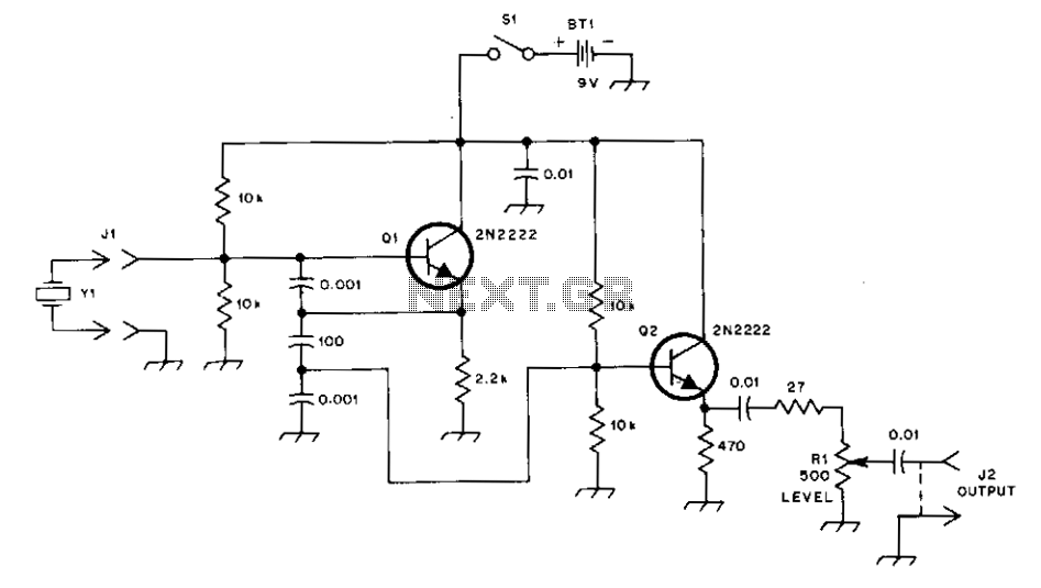
The described circuit serves as a versatile signal source, ideal for various applications in electronics testing and development, particularly in signal tracing. The Colpitts oscillator configuration is notable for its stability and ease of tuning, making it suitable for generating sine wave signals at desired frequencies within the specified range. The oscillator's frequency can be adjusted by selecting appropriate capacitors and inductors in the feedback network, allowing for fine-tuning to specific application needs.
The output stage employs a buffer amplifier, which is crucial for isolating the oscillator from the load. This isolation prevents loading effects that could alter the oscillator's performance. The use of an emitter follower configuration ensures that the output signal maintains the same voltage level while providing the necessary current drive capability.
The capacitive voltage divider serves a dual purpose: it attenuates the output voltage to a suitable level for the buffer amplifier while also maintaining the integrity of the signal. This is particularly important when interfacing with sensitive measurement equipment or when driving loads that require precise voltage levels.
Overall, this circuit design exemplifies an effective approach to generating stable and adjustable signal outputs, catering to the requirements of signal tracing and other related applications in electronic engineering. The careful selection of components and configuration ensures reliable operation across the specified frequency range, making it a valuable tool for engineers and technicians.This general purpose signal source serves very well in signal-tracing applications. The output level is variable to more than 1 Vrms into a 50 O load. Almost any crystal in the 1 to 15 MHz range can be used. Ql forms a Colpitis oscillator with the output taken from the emitter. A capacitive voltage divider (across the 2.2 emitter resistor) reduces the voltage applied to the buffer amplifier, Q2. The buffer and emitter follower, provides the low input impedance necessary to drive 50 O loads. 🔗 External reference
Related Circuits
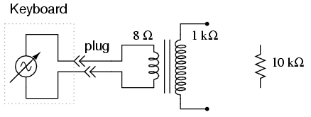
An electronic musical keyboard serves as a source of variable-frequency AC voltage signals. It is not necessary to purchase an expensive keyboard; a model with at least a few dozen voice selections (such as piano, flute, harp, etc.) is...

This article discusses various Teralab Electronics projects involving the 2N2222 transistor. The content is straightforward and informative. The components mentioned can enhance understanding of the projects detailed in this article. For instance, readers can find and purchase the 2N2222...
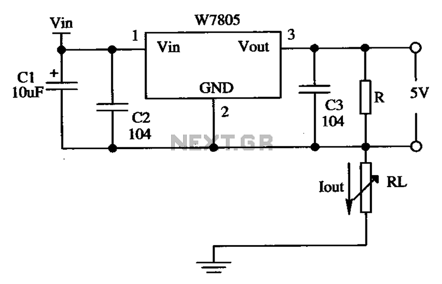
The circuit is composed of a W7805 positive current source application integration circuit that includes a voltage regulator. The W7805 regulator operates in suspension. A resistor is placed between its output terminal and the common terminal, forming a constant...
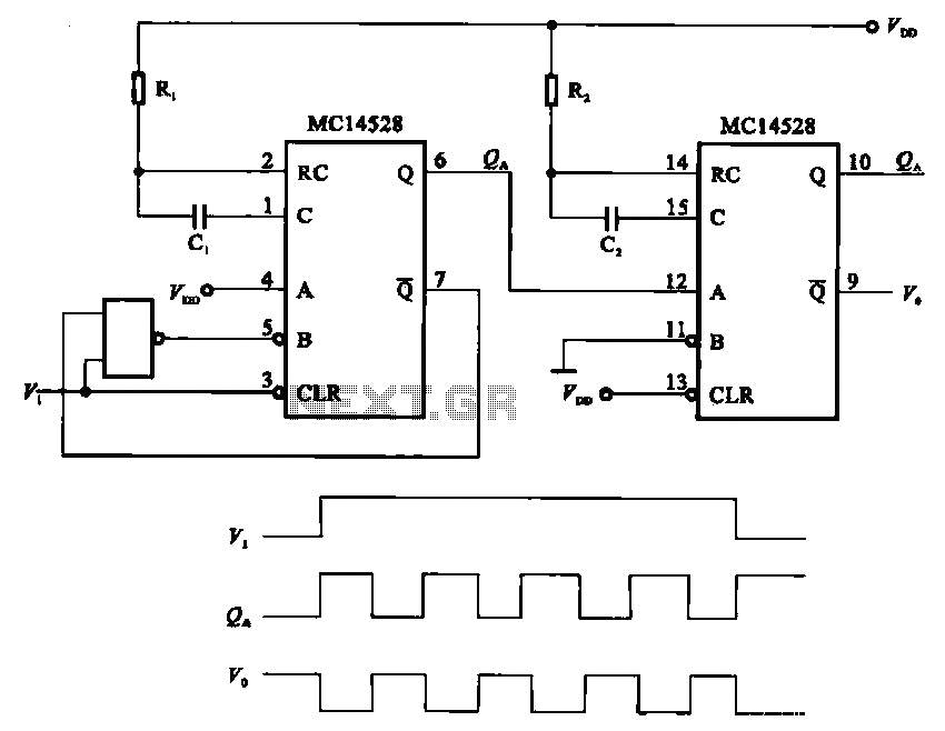
The pulse generating circuit monitors signals using monostable flip-flops. It generates a single-shot output signal based on the input pulse signal. A key signal from the monostable flip-flops is represented in a formula, with the input (V1) and output...

This is a simple high-frequency signal generator. By changing the inductance of the LC resonant circuit using the band switch S1, the high-frequency oscillation frequency range can be altered. The generator is divided into four frequency stages: the first...

A bridge sensor output signal precision differential instrumentation amplifier with adjustable gain IC1 amplified signal IS0100. The gain of IC1 is determined by the external resistor Rc. The IC2 current source output is sent to drive the bridge sensor,...