
Cute Palm-Sized DigiThermo
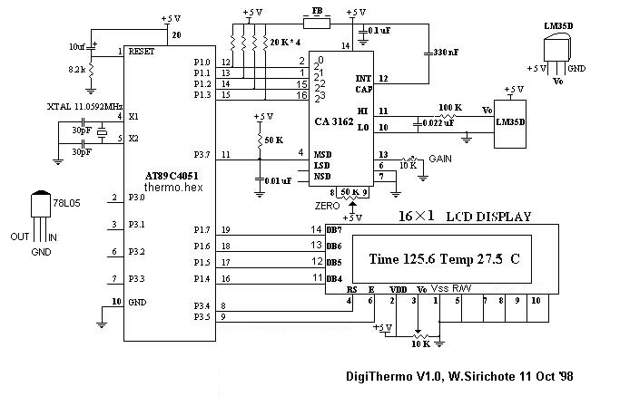
The A/D converter utilizes a dual-slope integrator to achieve a sampling rate of 10 Hz. The digital output sent to the microcontroller (MCU) is multiplexed in a four-bit Binary-Coded Decimal (BCD) format, starting from the Most Significant Digit (MSD), followed by the Least Significant Digit (LSD) and the Next Significant Digit (NSD), respectively.
The A/D converter operates based on the dual-slope integration method, which is known for its high accuracy and noise rejection capabilities. In this approach, the input analog voltage is integrated over a fixed time period, followed by a reverse integration of a reference voltage. This process effectively averages out noise and provides a stable output that is proportional to the input voltage.
The sampling rate of 10 Hz indicates that the converter takes one sample every 100 milliseconds. This rate is suitable for applications where rapid changes in the input signal are not expected, allowing for efficient data processing without overwhelming the MCU.
The digital output is formatted as a four-bit BCD, which encodes decimal digits in a binary format. This encoding is particularly useful for applications that require easy human readability or interfacing with digital displays. The multiplexing of the output signals ensures that the MCU can efficiently read each digit in sequence, starting with the MSD, which represents the highest place value, followed by the LSD and NSD. This method of output allows for a straightforward interpretation of the converted analog signal into a digital format suitable for further processing or display.
Overall, the design of this A/D converter with a dual-slope integrator and BCD output is well-suited for applications requiring precise analog-to-digital conversion while maintaining a manageable data rate for the microcontroller.The A/D converter employs dual-slope integrator providing 10Hz sampling rate, while Digital output sent to MCU will be multiplexing four bit BCD started from MSD, LSD and NSD respectively. 🔗 External reference
Related Circuits
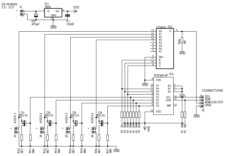
This page describes a battery tester designed to characterize batteries and save the results on a microSD card. The battery tester circuit is engineered to evaluate the performance and capacity of various battery types, providing accurate and reliable data storage...
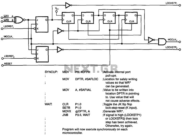
This hardware-software combination removes clocks from the slave until both integrated circuits synchronize. The firmware loop causes each circuit to generate a write (WR) signal once per loop. The circuit employs an exclusive-OR operation on the two WR signals...