
Dual 8051S Execute In Lock-Step
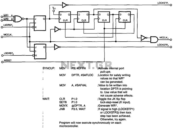
The described circuit functions as a synchronization mechanism for two integrated circuits (ICs), ensuring that they operate in unison by removing clock signals from the slave device until synchronization is achieved. The firmware loop plays a crucial role in generating a WR signal for each iteration, which is essential for monitoring the operational status of both ICs.
The exclusive-OR gate serves as a critical component, comparing the WR signals from both ICs. When there is a discrepancy between the two signals, the exclusive-OR gate outputs a miss-compare pulse. This pulse is vital as it triggers the JK flip-flops, which are designed to latch the state of the synchronization process. The outputs LOCKSTP1 and LOCKSTP2 indicate whether the ICs are in lock-step operation, which is characterized by both circuits executing their programs in sync.
In practical implementations using discrete components, it is recommended to connect to the Q output of the JK flip-flops. This approach simplifies the design by removing unnecessary inverters, thereby enhancing circuit efficiency. The use of ports 1 and 3 of the ICs for this configuration is strategic, ensuring that the necessary signals are accessible for proper synchronization.
It is important to note that utilizing a memory-mapped location for the lock-step-detect clear (K input) is not feasible due to the risk of generating additional WR signals, which could disrupt the synchronization process. Instead, employing the RD signals from the ICs can provide a more effective means of managing the lock-step-detect clear without interfering with the synchronization inputs, thus maintaining the integrity of the synchronization process. This design can be extended to other types of circuits, offering versatility in synchronization applications across various electronic systems. This hardware-software combination deletes clocks from the slave until both /iPs synchronize. The firmware loop causes each to generate a WR signal once per loop. The circuit exclusive-ORs the two WR signals to produce a miss-compare pulse. The miss-compare pulse latches into the two JK flip-flops via outputs LOCKSTP1 and LOCKSTP2. A high on these signals indicates that the /tPs are in lock-step, causing both juPs" programs" execution to exit the firmware loop. If you use discrete components, you"ll probably want to use the Q output of the JK flip-flop and delete the circuit"s inverters.
The listing uses the /iPs" ports 1 and 3. You cannot use a memory-mapped location for the lock-step-detect clear (K input) because this scheme would generate additional WR signals. You could apply this idea to other, perhaps using their RD signals. This way, generating an RD signal to activate the lock-step-detect clear would not affect the synchronization inputs.
🔗 External reference
Related Circuits
The TDA3567 is a monolithic integrated decoder designed for the NTSC color television standards. It incorporates all the necessary functions for the demodulation of NTSC signals. Additionally, it features a luminance amplifier and an RGB matrix amplifier. These amplifiers...
This circuit combines two separate line-level stereo (left and right) signals into a single stereo output, eliminating the need to switch between two sets of input signals. In this application, it is utilized to connect stereo audio from a...

A simple siren or alarm circuit utilizing the MC1458 dual op-amp and the audio power amplifier LM380 is presented. The circuit diagram includes various configurations for sirens, doorbells, and alarm systems, along with a comprehensive parts list. The circuit operates...
Here is a design for a DC motor speed control featuring: Efficient PWM H-bridge MOSFET architecture. Supply (battery) voltage range from 4.2 to 13 volts. High current capacity for driving large motors (65 amps max). Input compatible with standard...
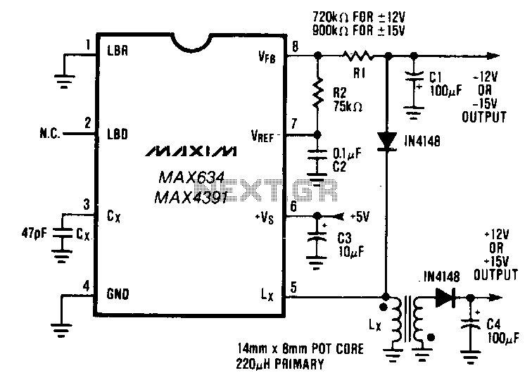
The buck-boost configuration of the MAX634 is well suited for dual output DC-DC converters. Only a second winding on the inductor is needed. Typically, this second winding is bifilar; the primary and secondary are wound simultaneously using two wires...
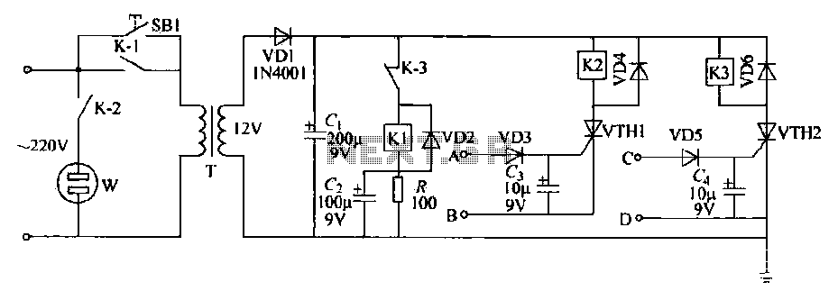
This schematic circuit features two alarm outputs controlled by a timer using thyristors. The system can be turned on or off and will shut down after the power supply is interrupted. It employs a transformer on the primary side...