
CW117 CW217 CW317 charger has a current-limiting protection configuration

The limiting protection charger circuit utilizes a combination of transistors and resistors to regulate the charging current supplied to a battery. The core component of this circuit is the VT transistor, which functions as a switch that activates when the charging current surpasses a predetermined threshold. Resistor R3 plays a critical role in this setup, as it is placed in series with the battery and is responsible for sensing the charging current.
When the charging current flows through R3, it generates a voltage drop across the resistor. This voltage drop is directly proportional to the charging current, following Ohm's law (V = I × R). If this voltage drop exceeds the threshold of 0.6V, the transistor VT becomes forward-biased and turns on. The conduction of VT effectively alters the circuit's characteristics by providing a lower resistance path in parallel with resistor R2. As a result, the overall equivalent resistance of the circuit decreases, which in turn leads to a reduction in the output voltage (Uo) and consequently limits the output current delivered to the battery.
The design of this circuit allows for flexibility in setting the maximum charging current by adjusting the value of resistor R3. For instance, if R3 is chosen to be 1 ohm, the maximum charging current can be calculated as Iom = 0.6V / 1Ω = 0.6A. However, if a smaller resistor value is selected, the charging current will increase, but it is crucial to ensure that this does not exceed the maximum output current rating specified for the integrated voltage regulator used in the circuit. This careful consideration of component values is essential for maintaining the integrity and safety of the battery charging process. Overall, the limiting protection charger circuit is an effective solution for preventing overcurrent conditions during battery charging, thereby enhancing the longevity and reliability of the battery. As shown in Figure is a limiting protection charger. VT transistors and resistors R3 form limiting network. Seen from the figure, the resistor R3 is the base of transistor VT e mitter Q resistor connected in series with the battery being charged. Charging current flows through the resistor R3. When the charge current is too large, the voltage drop on R3 exceeds 0.6V, the transistor VT will be turned on. Because VT parallel with resistor R2, VT conduction, so that the equivalent parallel resistance decreases, the output voltage Uo decreases, the output current is reduced, so as to achieve the purpose of limiting the charging current.
When taken R3 l ), the maximum charging current is Iom 0.6/1 0.6A, select a smaller R3 will be higher charging current, but can not exceed the maximum integrated voltage regulator output current value.
Related Circuits
The circuit schematic of the UDC consists solely of dispersive components. Two low-frequency series LC resonators, with equal inductances (LA=LB) and capacitances (CA=CB), are connected to two input semi-infinite transmission lines, designated as A and B. These resonators are...
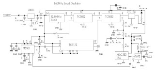
This 860 MHz Phase Locked Loop (PLL) oscillator circuit is designed for a 1200 MHz transverter's local oscillator with 435 MHz rigs. The oscillator utilizes Toshiba PLL synthesizer integrated circuits (ICs). The TC9122P serves as a preset counter for...

This circuit gives the sense of movement of a ball up and down, after the LEDs turn on successively, one after the other. As soon as it reaches one end or the other, it makes the opposite movement back....
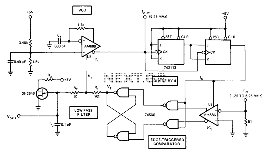
A circuit diagram of a phase-locked loop utilizes an AM686 latched comparator as a voltage-controlled oscillator, along with a TTL latch connected to generate edge-triggered comparators. The VCO and its comparison with the low-pass filter consisting of R1, R2,...
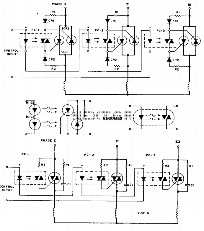
To simplify the following schematics and facilitate easy understanding of the principles involved, the following schematic substitution is used. Note that the triac driver is of limited use at 3-phase voltage levels. The following are three-phase switches for low...
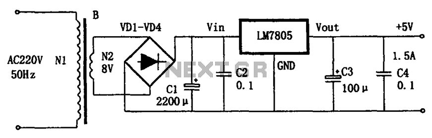
The circuit illustrated in the figure provides an output voltage of +5V and an output current of 1.5A. It comprises a power transformer, a bridge rectifier circuit consisting of diodes D1 to D4, and filter capacitor C1. Additionally, capacitors...