
DA-101 FM radio circuit chip
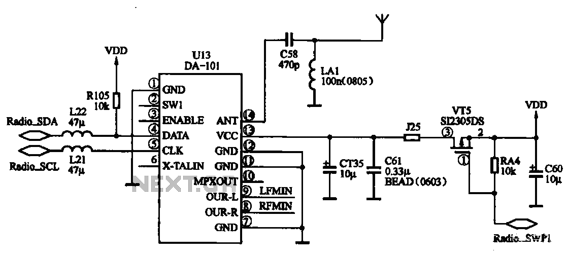
FM radio chip circuits, such as the one utilizing the DA-101 chip, are designed to receive and process FM radio signals effectively. The circuit operates by using a headset jack as an antenna, allowing for the capture of FM broadcasts. The initial signal captured is passed through coupling capacitor C58, which serves to filter and couple the radio frequency signal into the U13 chip.
Once the signal reaches U13, it undergoes several stages of processing. The first stage is high-frequency amplification, which boosts the strength of the received signal to ensure adequate processing. Following this, the signal is mixed, which involves combining it with a local oscillator frequency to convert it to an intermediate frequency (IF). This IF signal is then amplified further to improve clarity and reduce noise.
The output from pin U13 is the audio signal that has been demodulated from the original radio frequency carrier. This audio signal is directed to a digital decoder chip, which translates the audio data into a format suitable for playback or further processing. This integration of digital decoding allows for enhanced audio quality and compatibility with various playback devices.
Control of the radio circuit is managed by a CPU through the I2C bus interface. The CPU sends control signals, including data and clock signals, to the appropriate pins on U13 to facilitate operation. This digital communication allows for precise control over the radio's functions, such as tuning and volume adjustments.
Furthermore, the power management of the U13 chip is crucial for efficient operation. The CPU sends a control signal to gate VT5, which acts as a switch to manage the power supply to U13. By controlling VT5, the CPU can turn the power supply on or off, effectively managing the power consumption of the radio circuit and ensuring that it operates only when necessary. This design consideration enhances the overall efficiency and longevity of the FM radio circuit.Radio FM radio chip circuits use different, it works slightly different, as shown in the use of DA-101 chip FM Figure radio circuit. FM radio broadcast program in the state of the headset as an antenna jack FM radio circuit, the signal received by the antenna coupling capacitor c58 into the U13 @ feet. This signal is a radio frequency carrier. U13 carried out in high-frequency amplification, mixer, IF amplifier, frequency and other processing solutions to bring up the audio signal by , @ pin output, and then sent to a digital decoder chip for processing, radio circuit U13 k {JI as by CPU control, Izc bus control signal to the CPU (DATA, CLK) are applied to the U13 , feet.
Ul3 the radio power supply control signal is a control signal from the CPU applied to the gate VT5 by VT5 applied to the control power supply U13, so as to control the radio purposes.
Related Circuits
The battery voltage is 1V for a low-frequency amplifying circuit, which can operate with a power supply voltage ranging from 1V to 1.7V, making it suitable for use with small batteries. The circuit provides an output power of 80mW...
The BGl and BG2 form a directly coupled amplifier, while BG and BG4 consist of a monostable trigger circuit. Without receiving a prior trigger signal, BG3 enters a saturated conduction state. During this steady state, the collector of BG4...
The CMOS 4060 integrated circuit (IC) features two built-in inverters located at pins 9, 10, and 11, which must be interconnected to create an oscillator. The output of this oscillator is available at Pin 9, which continuously alternates between...
Using high-beam headlights can significantly enhance visibility while driving, but they can also pose a blinding hazard to other drivers. A simple circuit can be integrated into the headlight system to enable automatic switching between high and low beam...
A minimum number of parts yields a compact switching converter that can provide sufficient voltage to drive white LEDs. The resulting lamp is much more efficient, in terms of lumen hours per pound of battery, than incandescent bulbs, and...
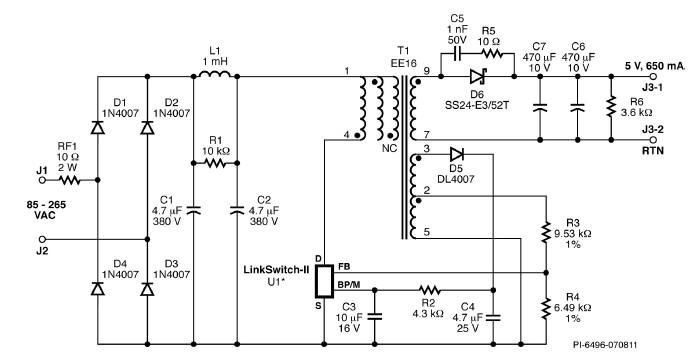
A simple 3.25W constant voltage/constant current (CV/CC) charger can be designed using the LinKSwitch family IC manufactured by Power Integrations. This electronic circuit project is intended to provide a 5-volt output with a maximum current of 650mA. The 3.25W...
Warning: include(partials/cookie-banner.php): Failed to open stream: Permission denied in /var/www/html/nextgr/view-circuit.php on line 713
Warning: include(): Failed opening 'partials/cookie-banner.php' for inclusion (include_path='.:/usr/share/php') in /var/www/html/nextgr/view-circuit.php on line 713