
CV/CC charger circuit diagram designed using LinKSwitch
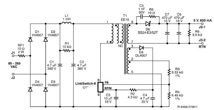
The described circuit is a compact and efficient solution for low-power charging applications. The LinKSwitch family IC serves as the core component, effectively managing the power conversion process while ensuring that the output remains stable under varying load conditions. The design utilizes a full-wave rectifier configuration with diodes D1 through D4, which converts the incoming AC voltage to a pulsating DC voltage. This rectified voltage is then smoothed out by the bulk capacitors C1 and C2, which serve to minimize voltage ripples and provide a stable DC output.
The inclusion of inductor L1 in conjunction with capacitors C1 and C2 forms a pi filter that is critical for reducing electromagnetic interference (EMI). This feature is particularly important in applications where sensitive electronic devices are present, as it helps to maintain compliance with EMI regulations and ensures reliable operation without interference.
The LinkSwitch-II IC, designated as U1 in the schematic, is a highly integrated solution that simplifies the design process. It combines several essential functions, including power switching, oscillation, and control, into a single package. This integration not only reduces the overall component count but also enhances the reliability of the circuit. The built-in 700V MOSFET provides adequate voltage headroom, allowing the charger to operate effectively across a wide range of input voltages, making it suitable for global applications.
Overall, this 3.25W CV/CC charger design exemplifies an efficient and reliable approach to power management, leveraging advanced semiconductor technology to deliver a stable output while minimizing size and complexity.A very simple 3. 25W CV/CC charger can be designed using LinKSwitch | family IC manufactured by Power Integrations. This electronic circuit project is designed to provide a 5 volts output at a maximum current of 650mA. This 3. 25W CV/CC charger, needs to be powered using a AC voltage between 85 and 265 VAC. The AC input power is rectified by dio des D1 through D4. Bulk storage capacitors C1 and C2 filter the rectified AC. Inductor L1 forms a pi ( ) filter with C1 and C2 to attenuate conducted differential-mode EMI noise. The LinkSwitch-II device (U1) incorporates the power switching device, an oscillator, a CC/CV control engine, startup circuitry, and protection functions into one IC. The integrated 700 V MOSFET allows sufficient voltage margin for universal input AC applications. 🔗 External reference
Related Circuits
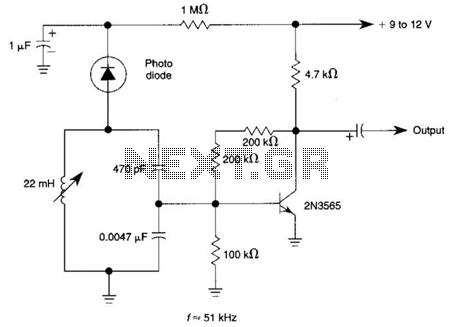
The circuit utilizes a tuned circuit for frequency selection, designed to operate at approximately 51 kHz. The 2N3565 transistor amplifies the output generated by the tuned circuit. The described circuit operates on the principle of resonance, where the tuned circuit...
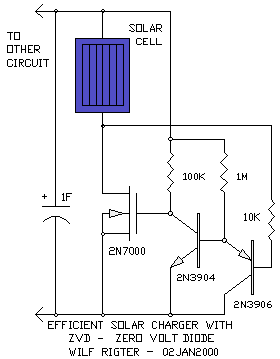
The Zero Volt Diode (ZVD) is a circuit useful in various applications, including solar chargers of all types. It is a novel circuit where a power MOSFET functions as a very low voltage drop diode, switching states at 0V...
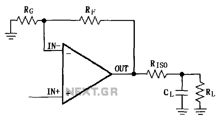
The MAX4223 to MAX4228 series incorporates a capacitive load drive circuit with an isolation resistor (RISO). The maximum allowable capacitive load for these devices is 25pF. However, exceeding this limit can lead to overshoot and ringing. The circuit design...
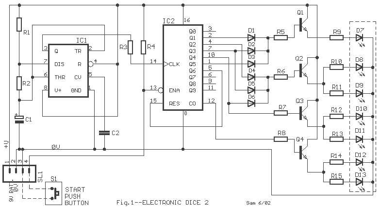
The IC1 is a 555 timer IC connected for astable operation. The clock pulses are fed to the IC2 via the 10K resistor. The IC2 is a 10-stage counter; output 6 (pin 5) is connected to RESET (pin 15),...
Using high-beam headlights can significantly enhance visibility while driving, but they can also pose a blinding hazard to other drivers. A simple circuit can be integrated into the headlight system to enable automatic switching between high and low beam...
The most elementary application is a half-wave control circuit. The thyristor is acting both as a power control device and as a rectifier, providing variable power to the load during the positive half cycle and no power to the...