
Design of VLSI Systems

Clock signals serve as the timing reference for digital circuits, coordinating operations within various components. The ideal characteristics of clock signals include rapid transitions (minimal rise and fall times), precise duty cycles (the ratio of the high state duration to the total period), and zero skew (the difference in arrival times of clock signals at different components). However, real-world implementations often face challenges such as non-zero skew and variable duty cycles, which can adversely affect the performance of digital systems.
In VLSI chip design, the generation of reliable clock signals is vital. Ring oscillators, while simple and effective for generating primary clock signals, can introduce instability due to their dependence on manufacturing processes. As a result, high-performance applications typically rely on dedicated clock chips that utilize crystal oscillators, which provide improved frequency stability.
The Pierce crystal oscillator is a widely used circuit configuration that achieves stable oscillation through a series-resonant approach. The crystal's behavior can be modeled as a series RLC circuit, where the internal resistance influences the oscillation frequency. The load impedance at the crystal's terminals also plays a significant role in determining both frequency and stability, necessitating careful design considerations.
In VLSI applications, clock distribution networks must be designed to minimize skew. Techniques such as H-tree structures and local skew balancing are employed to ensure uniform distribution of clock signals. Additionally, advanced computer-aided design tools can optimize the layout of clock distribution networks to achieve zero skew. Buffering is essential to manage fan-out loads, and each buffer stage should maintain balanced delays to ensure synchronous operation across the chip.
In high-performance designs, maintaining equal interconnect lengths and implementing extensive buffering are critical strategies for achieving reliable clock signal distribution. The use of mesh patterns with cross-connected interconnect wires further enhances phase stability across the chip, which is paramount for high-speed operations. Overall, the design and implementation of clock signal circuits and distribution networks are fundamental to the performance and reliability of modern digital systems.Clock signals are the heartbeats of digital systems. Hence, the stability of clock signals is highly important. Ideally, clock signals should have minimum rise and fall times, specified duty cycles, and zero skew. In reality, clock signals have nonzero skews and noticeable rise and fall times; duty cycles can also vary.
In fact, as much as 10% of a machine cycle time is expended to allow realistic clock skews in large computer systems. The problem is no less serious in VLSI chip design. A simple technique for on-chip generation of a primary clock signal would be to use a ring oscillator as shown in Fig. 5. 1. Such a clock circuit has been used in low-end microprocessor chips. However, the generated clock signal can be quite process-dependent and unstable. As a result, separate clock chips which use crystal oscillators have been used for high- performance VLSI chip families.
Figure 5. 2 shows the circuit schematic of a Pierce crystal oscillator with good frequency stability. This circuit is a near series-resonant circuit in which the crystal sees a low load impedance across its terminals. Series resonance exists in the crystal but its internal series resistance largely the determines the oscillation frequency.
In its equivalent circuit model, the crystal can be represented as a series RLC circuit; thus, the higher the series resistance, the lower the oscillation frequency. The external load at the terminals of the crystal also has a considerable effect on the frequency and the frequency stability.
The inverter across the crystal provides the necessary voltage differential, and the external inverter provides the amplification to drive clock loads. Note that the oscillator circuit presented here is by no means a typical example of the state-of-the-art; design of high-frequency, high-quality clock oscillators is a formidable task, which is beyond the scope of this section.
Usually a VLSI chip receives one or more primary clock signals from an external clock chip and, in turn, generates necessary derivatives for its internal use. It is often necessary to use two non-overlapping clock signals. The logical product of such two clock signals should be zero at all times. Figure 5. 3 shows a simple circuit that generates CK-1 and CK-2 from the original clock signal CK. Figure 5. 4 shows a clock decoder circuit that takes in the primary clock signals and generates four phase signals.
The reduction of clock skews, which are caused by the differences in clock arrival times and changes in clock waveforms due to variations in load conditions, is a major concern in high-speed VLSI design. In addition to uniform clock distribution (H-tree) networks and local skew balancing, a number of new computer-aided design techniques have been developed to automatically generate the layout of an optimum clock distribution network with zero skew.
Figure 5. 6 shows a zero-skew clock routing network that was constructed based on estimated routing parasitics. Regardless of the exact geometry of the clock distribution network, the clock signals must be buffered in multiple stages as shown in Fig.
5. 7 to handle the high fan-out loads. It is also essential that every buffer stage drives the same number of fan-out gates so that the clock delays are always balanced. In the configuration shown in Fig. 5. 8 (used in the DEC Alpha chip designs), the interconnect wires are cross- connected with vertical metal straps in a mesh pattern, in order to keep the clock signals in phase across the entire chip.
So far we have seen the needs for having equal interconnect lengths and extensive buffering in order to distribute clock signals with minimal skews andratio of the line width to vertical separation distanc 🔗 External reference
Related Circuits
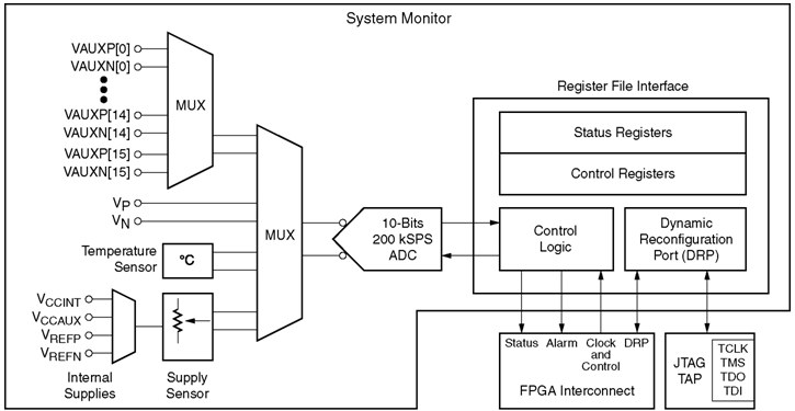
The System Monitor feature discussed in this article was successfully utilized by Avalon Microelectronics in two Virtex-5 FPGAs (XC5VLX330T) during their development. They encountered an unusual issue where the development board would shut down while the FPGAs were executing...
The power supply unit (PSU) in question does not appear to be exceptionally large. Eagle software should be capable of managing these dimensions. The focus was more on finding an alternative that may already include the necessary components and...
A single IC 556 has been utilized to generate PWM pulses. One half of the IC is configured as a high-frequency generator, which supplies the other half of the IC, set up as a pulse width modulator. The modulating...
The problem with class-B amplifier design is that we start with an output stage in two halves, each with a non-linear response, which we then add together to try to give a linear response, i.e. so that a graph...
This article is intended for individuals interested in constructing their own car amplifier. The fundamental calculations involved will be discussed below. Understanding these concepts will enable the construction of a car amplifier independently. The complexity of designing a car...
Datagoo is based on the ATMEGA328P microcontroller, widely used by hobbyists in various Arduino projects. It can be programmed via any computer with a USB port when paired with an FTDI FT232RL USB-Serial circuit. Cost-effectiveness and simplicity were prioritized...