Differential Amplifiers
1. Definition and Purpose
1.1 Definition and Purpose
Differential amplifiers are integral components in the realm of analog electronics, serving as critical building blocks for a variety of applications including instrumentation, signal processing, and the amplification of sensor outputs. At their core, a differential amplifier amplifies the difference between two input voltages while rejecting any signals that are common to both inputs. This unique ability to enhance the desired signal while minimizing noise and interference makes differential amplifiers exceptionally valuable in real-world applications where precision is paramount.
To delve deeper, we can start by defining their operation mathematically. A basic differential amplifier can be described by the equation:
In this expression, \( V_{\text{out}} \) represents the output voltage, \( A_d \) is the differential gain, and \( V_2 \) and \( V_1 \) are the voltages at the non-inverting and inverting inputs, respectively. The differential gain \( A_d \) is a critical parameter that determines how effectively the amplifier can transform the input voltage difference into a measurable output.
The purpose of employing differential amplifiers extends far beyond simple amplification. These devices excel in applications where signal integrity is compromised by noise, such as in medical instrumentation (e.g., electrocardiograms), industrial sensors, and audio processing. For instance, in an electrocardiogram (ECG) system, differential amplifiers allow for the collection of weak electrical signals produced by the heart, while simultaneously rejecting noise generated by surrounding electronic devices. This capability is essential for accurate diagnostics and monitoring in clinical settings.
Historically, differential amplifiers have evolved significantly from their initial implementations using discrete components to modern integrated circuit designs that facilitate enhanced performance metrics. The emergence of operational amplifiers (op-amps), which are essentially high-performance differential amplifiers, has broadened the scope of their application, allowing for more sophisticated signal processing tasks to be executed with ease.
In learning about differential amplifiers, it's crucial to understand both their theoretical foundations and practical implementations. As we progress through this tutorial, we will explore various types of differential amplifiers, their configurations, and how their characteristics can be optimized for specific applications. By solidifying this foundational knowledge, readers will be better equipped to leverage differential amplifiers in advanced electronic systems, enhancing both performance and reliability.
1.2 Applications in Electronics
Differential amplifiers are crucial components in a variety of electronic circuits and systems, serving to enhance signals while reducing noise and interference. This property makes them indispensable in several applications across communications, medical instrumentation, and data acquisition systems, among others.
Signal Processing
In communications, differential amplifiers are employed in modulation and demodulation processes. For instance, they are integral to phase-shift keying (PSK) and frequency-shift keying (FSK) systems where the goal is to accurately recover transmitted signals from amid noise. By only amplifying the difference between two input signals, they ensure that common-mode noise is significantly rejected, thereby enhancing fidelity in signal transmission.
Medical Instrumentation
Differential amplifiers find extensive use in biomedical applications. For example, electrocardiograms (ECGs) and electroencephalograms (EEGs) utilize these amplifiers to measure small voltage changes due to physiological activities. Since these signals are often on the order of microvolts and can be easily drowned out by noise, differential amplifiers are critical for improving the signal-to-noise ratio (SNR), allowing for accurate readings of the heart's electrical activity or brainwaves.
Data Acquisition Systems
In data acquisition systems, differential amplifiers serve to condition analog signals before they are converted to digital form. They enable the measurement of voltage differences across components in a circuit, such as strain gauges or temperature sensors, where precise readings are essential. A clear example is the use of differential amplifiers in load cells to accurately measure weight based on the output voltage caused by deformation in the sensor's material.
Operational Amplifier Circuits
Differential amplifiers are also widely utilized in operational amplifier (op-amp) circuits. The inverting and non-inverting configuration of op-amps takes advantage of differential input behavior for tasks such as signal attenuation, summation, and comparator applications. This versatility underscores their importance in analog circuit design.
Instrumentation Amplifiers
Instrumentation amplifiers, which are built using multiple differential amplifiers, are specifically designed to have high input impedance and excellent common-mode rejection. These characteristics make them suitable for precise measurements in industrial settings, such as monitoring electrical sensors where even minimal interference can impact performance.
Summary
In summary, differential amplifiers are foundational to numerous applications in electronics. Their ability to isolate the signal of interest from noise ensures that they play a pivotal role in advancing technology across various fields. As electronic systems continue to evolve, the significance of differential amplifiers will only increase, paving the way for new innovations in processing and measurement techniques.
2. Common-Mode and Differential Signals
2.1 Common-Mode and Differential Signals
In the realm of differential amplifiers, understanding the distinction between common-mode and differential signals is paramount. These two signal types play a critical role in the operation of differential amplifiers, influencing their performance in various applications, particularly in environments filled with noise and interference.
Common-mode signals refer to voltages that are present equally on both inputs of the amplifier. In practical scenarios, these signals often arise from external noise or interference, affecting both input lines uniformly. For example, if both input voltages are subject to the same noise from an external electromagnetic interference source, that noise would be classified as a common-mode signal. As one delves deeper into circuitry design, recognizing common-mode signals becomes crucial for enhancing the signal integrity in communication systems.
Conversely, differential signals are defined by their disparities between the two inputs. The differential signal, denoted as \( V_{diff} \), is the difference in voltage between the two input terminals:
This signal is what differential amplifiers are primarily designed to amplify, while ideally rejecting any common-mode signals. The ability to effectively sense and amplify these differences is vital in applications ranging from audio processing to instrumentation and medical devices.
To gain a better grasp of this concept, one can visualize it as follows: imagine two parallel waveforms representing the input voltages. The common-mode signal would appear as a uniformly shifted waveform, while the differential signal would represent the variations or fluctuations occurring between the two inputs. This visualization is crucial as it lays the groundwork for understanding how differential amplifiers perform signal processing tasks.
This understanding is not merely theoretical; it has practical implications in the design of various electronic systems. In operational amplifiers and instrumentation amplifiers, high common-mode rejection ratios (CMRRs) are desired to ensure that the differential signal is extracted reliably while minimizing the impact of common-mode signals.
Ultimately, realizing the interaction between common-mode and differential signals equips engineers and researchers with the tools needed to design and implement more effective signal-processing systems. This knowledge is fundamental to optimizing performance in noisy environments, an aspect increasingly critical in modern electronic communications systems.
As we proceed, the next section will delve into the configuration of differential amplifiers, laying the groundwork for understanding their design and application in various circuits.
2.2 Basic Configuration and Signal Flow
Differential amplifiers are integral components in many electronic applications, serving a wide range of purposes from audio processing to instrumentation. Understanding the basic configuration and signal flow within these amplifiers is critical for harnessing their full potential in complex electronic systems. This subsection delves into the fundamental architecture, operational principles, and relevant applications of differential amplifiers.
Basic Configuration
The differential amplifier essentially amplifies the difference between two input signals while rejecting any voltage common to both inputs. Its foundational configuration typically consists of four main components:
- Two input resistors (R1 and R2): These resistors are connected to the two input terminals, generally denoted as Vin+ and Vin-.
- Two feedback resistors (R3 and R4): They connect the output (Vout) back to the inverting input terminal to form the feedback loop.
- The operational amplifier (op-amp): This crucial component serves to magnify the voltage difference between its inputs.
- Power supply: Essential for providing the necessary operating voltage for the op-amp.
In this configuration, the op-amp is designed to establish high input impedance and low output impedance, limiting the effect on the signal source while allowing easy interfacing with subsequent stages in a signal chain.
Signal Flow and Operation
The signal flow in a differential amplifier can be understood through the equation governing its output:
Where:
- Vout: Output voltage of the amplifier.
- Vin+: Voltage at the non-inverting terminal.
- Vin-: Voltage at the inverting terminal.
- R3 and R4: Feedback resistors that influence the gain.
To derive this output equation, we can analyze the operating principles embodied within the differential amplifier geometry. Using Kirchhoff’s laws, we can set up equations based on the input terminal relationships as follows:
1. Applying KCL at the inverting terminal: $$ \frac{V_{in-} - V_{out}}{R_4} + \frac{V_{in-}}{R_3} = 0 $$ 2. Rearranging gives: $$ V_{out} = V_{in-} \left( \frac{R_4}{R_3} \right) $$ 3. Similarly, applying KCL at the non-inverting terminal yields: $$ V_{out} = V_{in+} - V_{in-} \left( \frac{R_4}{R_3} \right) $$ 4. By equating the two expressions for \( V_{out} \): $$ \left( \frac{R_4}{R_3} \right) V_{in+} - \left( \frac{R_4}{R_3} \right) V_{in-} = V_{out} $$ 5. This concludes the derivation and emphasizes the role of feedback resistors in providing gain to the differential input.The practical applications of differential amplifiers span various domains, from precision measurement systems in biomedical devices to instrumentation for industrial control systems. In audio technology, differential amplifiers help to eliminate unwanted noise, ensuring clarity and fidelity in sound reproduction.
Overall, mastery over differential amplifier configurations and signal flow lays the groundwork for their applications in real-world scenarios, reinforcing their significance across various engineering and scientific disciplines.
2.3 Ideal vs. Real Differential Amplifiers
Differential amplifiers serve as fundamental building blocks in various electronic applications, from signal processing to data acquisition systems. While the ideal differential amplifier forms a theoretical model characterized by infinite input impedance, zero output impedance, and infinite common-mode rejection ratio (CMRR), real-world implementations exhibit limitations due to non-ideal characteristics. Understanding the differences between ideal and real differential amplifiers allows engineers to make informed design decisions, especially when striving for reliable performance in practical applications.
Ideal Differential Amplifier Characteristics
The ideal differential amplifier is defined by a few key characteristics:
- Infinite Input Impedance: This implies that no current flows into the amplifier inputs, allowing for accurate voltage representation of the inputs.
- Zero Output Impedance: An ideal differential amplifier can drive any load without affecting the output voltage.
- Infinite Common-Mode Rejection Ratio (CMRR): This characteristic ensures that any voltage common to both inputs does not affect the output, making the amplifier immune to noise and fluctuations present in both input signals.
The behavior of an ideal differential amplifier can be described mathematically using the following equation, where the output voltage (\( V_{out} \)) is proportional to the difference between the input voltages (\( V_{in+} \) and \( V_{in-} \)):
where \( A_d \) is the differential gain.
Real Differential Amplifier Limitations
Transitioning from the ideal to real-world scenarios, engineers encounter several limitations that affect the performance of real differential amplifiers:
- Finite Input Impedance: Real amplifiers possess finite input impedance, which leads to loading effects that can distort the input signals, ultimately lowering the voltage accuracy.
- Non-Zero Output Impedance: This introduces a voltage drop when driving loads, which can significantly impact performance, especially in precision applications.
- Limited CMRR: Real devices exhibit reduced common-mode rejection due to mismatches within the amplifier components, allowing common-mode signals and noise to be amplified.
- Offset Voltage: A small voltage difference exists even when the inputs are equal, leading to undesired output voltages.
- Temperature Drift: Component parameters can change with temperature variation, influencing biasing and gain characteristics.
Implications in Applications
In practical applications, the understanding of these limitations allows engineers to design circuits more resilient to noise and other unwanted signals. For instance:
- Instrumentation Amplifiers: These devices exploit differential amplifiers to achieve high gains with low noise, compensating for the finite CMRR through careful design and component matching.
- Common-Mode Feedback Circuits: Such circuits can be employed to improve the CMRR and mitigate the effects of common-mode signals in high-frequency applications.
Therefore, while ideal differential amplifiers serve as a useful abstraction for theoretical analysis, practical considerations are essential for effective circuit design. Recognizing the constraints of real differential amplifiers paves the way for engineering solutions that harness their advantages while mitigating shortcomings.
3. Voltage Gain Derivation
3.1 Voltage Gain Derivation
The differential amplifier is a fundamental building block in analog electronics, widely utilized in applications such as operational amplifiers, instrumentation amplifiers, and data acquisition systems. To accurately assess its performance, one of the key parameters to analyze is the voltage gain. This subsection will provide a detailed derivation of the voltage gain for a standard differential amplifier configuration, emphasizing both theoretical considerations and practical implications.
In a typical differential amplifier setup using bipolar junction transistors (BJTs) or field-effect transistors (FETs), we represent the input voltages as V1 and V2, corresponding to the two inputs of the amplifier. The main objective is to derive the voltage gain, Av, which is defined as the ratio of the output voltage Vout to the difference of the input voltages:
This formula indicates that the voltage gain is dependent on how effectively the amplifier can amplify the difference between its input signals. To proceed with the derivation, we will consider the following assumptions for the general case of a differential pair configuration:
- The transistors are matched, meaning their parameters are identical.
- The input common-mode voltage has minimal effect on the differential gain.
- The output is taken differentially with respect to the ground reference.
For BJTs in a typical differential amplifier, let us denote the transconductance as gm, and the output resistance of each transistor as ro. The output voltage can be expressed in terms of the transconductance and the output resistance:
Considering the voltage drop across the output resistance, we can plug this expression back into our original definition of voltage gain:
This result shows that the voltage gain of a differential amplifier can be simplified to the product of transconductance and output resistance, emphasizing the importance of these parameters in defining the amplifier’s performance. In practical scenarios, this means that increasing the transconductance, perhaps through the use of high-quality semiconductor materials or through circuit design techniques, can effectively enhance the voltage gain.
Moreover, it's worth mentioning the significance of the common-mode rejection ratio (CMRR) in applications: while a high voltage gain is desirable, it is equally important to ensure that the amplifier rejects common-mode signals, thus retaining accuracy in the presence of noise. This balance is critical in applications ranging from sensor interfaces to audio equipment, where maintaining signal integrity amidst external interference is paramount.
3.2 Input and Output Impedance
Differential amplifiers play a pivotal role in the realm of analog electronics, particularly in signal processing applications. They are characterized by their ability to amplify the voltage difference between two input signals while rejecting any signals that are common to both inputs, known as common-mode signals. Understanding the input and output impedances of differential amplifiers is critical for optimizing their performance within electronic circuits.
Input impedance refers to the impedance presented by the amplifier to the input source. It is essential for maximizing voltage transfer from the source to the amplifier and minimizing the loading effect that may distort the intended signal. Conversely, the output impedance defines how the amplifier interacts with the connected load. A low output impedance is generally desired to ensure effective coupling to the next stage of the circuit, thereby enhancing the amplifier's ability to drive loads without significant voltage drop.
Input Impedance
The input impedance of a differential amplifier can be influenced primarily by the configuration of the input stage, typically comprising transistors or operational amplifiers. For a basic differential amplifier using an operational amplifier (op-amp), the input impedance can be expressed largely in terms of the resistors used at the input.
Consider a differential op-amp configuration where two resistors, \( R_1 \) and \( R_2 \), connect the differential inputs to the ground. The input impedance for each of these inputs can be approximated as:
where \( A_{v} \) is the voltage gain of the amplifier. In scenarios where the gain is substantially large relative to the resistors, this can lead to a very high input impedance. For differential amplifiers constructed with high-value resistors and active devices like JFETs or MOSFETs, input impedances can reach the mega-ohm range, enabling the amplifier to accept weak signals with minimal loading.
Output Impedance
Output impedance, on the other hand, is crucial for determining how much the output voltage will vary with different load conditions. Ideally, for effective signal transfer, the output impedance should be low. In practical applications, when an output stage of a differential amplifier is connected to a load resistor, the output impedance can be represented as:
Here, \( r_{o} \) represents the output resistance of the amplifier, while \( R_{L} \) denotes the load resistance. In perfect scenarios, the output impedance is minimized to ensure that even with the load connected, the amplifier maintains a stable output close to its design voltage. When the output impedance is higher, it can lead to voltage drops across the output stage, which can distort the amplified signal, leading to degradation in performance.
Practical Relevance
Understanding input and output impedance configurations helps engineers effectively design differential amplifiers for various applications, including:
- Audio processing systems where maintaining a clear signal is essential.
- Instrumentation applications that require accurate measurements with high input impedance to avoid impacting the measurement results.
- Communication systems, where differential signaling contributes to enhanced noise immunity, making impedance consideration critical for performance.
Ultimately, optimizing the input and output impedances can significantly enhance the functionality and reliability of differential amplifiers in real-world applications. A deep consideration of these parameters not only amplifies signals effectively but also safeguards the integrity of data transmission across electronic systems.
3.3 CMRR (Common-Mode Rejection Ratio) Calculation
The Common-Mode Rejection Ratio (CMRR) is a critical parameter for differential amplifiers, indicating how effectively the amplifier can reject common-mode signals while amplifying differential signals. It is particularly vital in applications involving noise reduction, such as in instrumentation amplifiers or audio processing, where external interference can significantly degrade signal integrity.
CMRR is defined mathematically as the ratio of the differential gain (Ad), which amplifies the difference between the two input signals, to the common-mode gain (Ac), which amplifies signals that are present simultaneously on both inputs. Mathematically, this can be expressed as:
To compute CMRR accurately, we need to derive expressions for both the differential gain (Ad) and the common-mode gain (Ac). Let's explore these derivations step-by-step, starting from the basic configurations of a differential amplifier.
Differential Gain (Ad)
The differential gain can typically be expressed in terms of resistor values in a standard operational amplifier setup. Consider two input resistors, R1 and R2, and feedback resistors, Rf1 and Rf2. The relationship for differential gain is given by:
Where Rf is the effective feedback resistor, and R is the equivalent input resistor connected to the input where the differential signal is applied. In an ideal differential amplifier, this gain is maximized by proper selection of resistor values.
Common-Mode Gain (Ac)
In contrast, the common-mode gain can be expressed similarly, but it incorporates both the input resistors and the feedback path, considering that both inputs receive the same signal. The common-mode gain can often be approximated as:
Where R_{in} is the input impedance of the operational amplifier, and "∥" refers to the parallel combination of resistances. This relationship reveals how sensitive the operational amplifier is to common-mode signals.
Calculating CMRR
Substituting the expressions for Ad and Ac into the formula for CMRR gives us:
This equation ultimately shows that optimal CMRR can be achieved through careful design and matching of resistors. For linear applications, ensuring that the resistors are closely matched increases the CMRR, thus improving the amplifier's ability to reject unwanted common-mode signals.
Practical Relevance
For engineers and designers, understanding CMRR is fundamentally important for applications like audio amplifiers, sensor signal processing, and communication systems where any unwanted signals can seriously affect the performance and clarity of data transmission. By focusing on achieving a high CMRR, we can ensure that our differential amplifiers maintain signal fidelity even in noisy environments.
To conclude, the Common-Mode Rejection Ratio is a vital performance metric that can greatly influence the effectiveness of differential amplifiers in real-world applications. Continually optimizing this parameter should be a primary goal for both research initiatives and practical circuit designs.
4. Component Selection
4.1 Component Selection
The selection of components for differential amplifiers is critical to achieving the desired operational characteristics and performance metrics. Engineers must consider various parameters such as gain, bandwidth, input and output impedances, noise performance, and power consumption. Each component plays a distinct role, and their interrelationships greatly influence the overall behavior and efficacy of the amplifier. This section delves into the critical components that constitute differential amplifiers, including operational amplifiers, resistors, capacitors, and transistors.
Operational Amplifiers
At the heart of many differential amplifiers lies the operational amplifier (op-amp). Key Characteristics:
- Input Impedance: A high input impedance is crucial to prevent loading effects that could alter the input signal.
- Common-Mode Rejection Ratio (CMRR): A high CMRR ensures that common noise signals are effectively rejected, allowing for clear differentiation between the two input signals.
- Open-Loop Gain: The open-loop gain of an op-amp impacts the overall gain structure of the amplifier.
Commonly used op-amps in differential amplifier designs include the LM358, TL072, and AD620. The choice of op-amp should align with the specific requirements of the application, such as low noise for audio applications or high-speed for RF applications.
Resistors
Resistors play a crucial role in defining the gain and input impedances of differential amplifiers. The resistor values in the feedback loop directly affect the gain, and their tolerance can significantly impact performance. Considerations for Resistor Selection:
- Value: Choose resistors that provide the desired gain according to the equation $$ V_{out} = (R_f / R_{in}) V_{in} $$ where $$ R_f $$ is the feedback resistor and $$ R_{in} $$ is the input resistor.
- Tolerance: Low-tolerance (<1%) resistors minimize variations in gain and enhance circuit predictability.
- Temperature Coefficient: Select resistors with low temperature coefficients to maintain constant performance across varying temperatures.
Capacitors
Capacitors are utilized primarily for AC coupling and signal stabilization in differential amplifier circuits. Their role is to filter out noise and prevent DC offsets from affecting the performance. Selection Criteria:
- Type: Ceramic capacitors are often preferred for high-frequency applications due to their low equivalent series resistance (ESR) and self-resonant frequency.
- Value: Capacitance values must be selected to accommodate the frequency response of the signals being amplified and to ensure that phase shifts are minimized.
Transistors
In instances where discrete components are favored over integrated options, bipolar junction transistors (BJTs) or field-effect transistors (FETs) may be used to build differential amplifiers. These components characteristically offer high gain and low noise. Considerations for Transistor Selection:
- Type: BJTs are generally preferred for low-noise operations while FETs are favored in high-impedance applications.
- Current Gain: The transistor's Beta parameter, $$\beta$$, should be adequately high to ensure amplification is reached efficiently.
- Bandwidth: Evaluate the transition frequency (fT) to ensure that the amplifier can effectively operate at the desired signal frequency.
Understanding the intricacies of component selection for differential amplifiers not only enhances theoretical knowledge but is also paramount in practical circuit design. The implications of undesirable component interactions can lead to compromised performance, noise susceptibility, or even complete circuit failure. Thus, careful consideration should always guide the selection process, balancing performance against practical constraints such as cost and availability.
4.2 Feedback Mechanisms
In the analysis of differential amplifiers, feedback mechanisms play a crucial role in determining both the functionality and stability of the circuit. Feedback can be categorized into two main types: positive feedback and negative feedback. Understanding these mechanisms is essential for enhancing performance characteristics such as gain, bandwidth, and linearity.
Negative Feedback
Negative feedback is often employed in amplifier circuits to improve stability and reduce distortion. In a differential amplifier, negative feedback occurs when a portion of the output is fed back to the inverting input. This mechanism effectively reduces the overall gain of the amplifier while enhancing linearity and bandwidth.
To illustrate the effect of negative feedback mathematically, consider a basic differential amplifier configuration with gain \( A \). The output voltage \( V_{\text{out}} \) is given by:
When negative feedback is applied, the output voltage is sampled and a fraction \( \beta \) is fed back to the inverting input. The modified input to the inverting terminal is thus \( V_- + \beta V_{\text{out}} \). The new expression for the output voltage becomes:
Rearranging and solving for \( V_{\text{out}} \) yields the feedback formula:
This equation shows that the effective gain of the amplifier is now \( \frac{A}{1 + A\beta} \), which decreases as \( \beta \) increases. This illustrates the stabilizing effect of negative feedback, as increased feedback results in a more controlled amplifier performance, making it less susceptible to variations in component values or outside disturbances.
Positive Feedback
In contrast, positive feedback can be employed in applications requiring aggressive amplification or switching behavior, such as in oscillators or certain comparator circuits. In this scenario, feedback from the output enhances the input signal at the same polarity, potentially leading to instability because it can result in saturation conditions. In other words, while negative feedback causes the output to diminish the input signal, positive feedback magnifies it, leading to positive loop gain.
The challenge with positive feedback in differential amplifiers is to manage the balance between achieving the desired amplification and preventing the circuit from oscillating uncontrollably. By applying controlled positive feedback, one might achieve specific characteristics such as faster response times or increased sensitivity in detecting small signals.
Practical Applications
The applications of feedback mechanisms in differential amplifiers can be seen across various fields:
- Instrumentation amplifiers: Here, negative feedback helps maintain high input impedance while providing stable gain, crucial in sensor applications where signal fidelity is essential.
- Operational amplifiers: These devices frequently employ both types of feedback to balance performance requirements, allowing for precise control over gain while minimizing offset errors.
- ADC and DAC interfaces: Feedback mechanisms can ensure that differential signals are accurately processed, maintaining signal integrity throughout the conversion process.
Understanding and effectively utilizing feedback mechanisms is crucial for engineers and researchers aiming to design robust differential amplifiers tailored to their specific applications. The balance of stability, gain, and responsiveness ensures that these circuits can produce reliable performance in a variety of settings.
4.3 Noise Reduction Techniques
In the design and application of differential amplifiers, noise can significantly affect performance, particularly in sensitive electronic applications. This section elaborates on advanced techniques for reducing noise, which often involves both the optimization of circuit design and the implementation of specific strategies aimed at minimizing extraneous signals.
Understanding Noise in Differential Amplifiers
To appreciate noise reduction techniques, it is vital to first comprehend the sources and types of noise that can affect differential amplifiers. Common noise sources include thermal noise, shot noise, flicker noise, and burst noise. Each of these noise categories has different characteristics and impacts on the signal, often determined by both the components used and the configuration of the amplifier.
Identifying Key Noise Sources
Thermal noise, generated by the random motion of charge carriers within resistors, is temperature-dependent and unavoidable in practical circuits. The noise current can be expressed by the Johnson-Nyquist formula:
where k is Boltzmann's constant, T is the absolute temperature in Kelvin, and R is the resistance in ohms. This formula highlights that reducing resistance or operating at lower temperatures can effectively mitigate thermal noise.
Noise Reduction Techniques
Several strategies are employed to combat noise in differential amplifiers, which can be categorized into design choices, component selection, and shielding methods:
- Common-Mode Rejection Ratio (CMRR): Optimizing CMRR is central to noise reduction. Employing matched components in the amplifier can enhance the ability to reject common-mode signals, emphasizing the desired difference signal over noise.
- Low-Noise Components: Selecting low-noise resistors, operational amplifiers, and transistors can play a pivotal role in reducing the overall noise floor of the circuit. Components such as metal film resistors are preferred for their low noise characteristics.
- Feedback Techniques: Implementing negative feedback not only stabilizes gain but can also reduce the effects of noise by improving linearity and effective bandwidth.
- Shielding and Grounding: Proper shielding of the amplifier inputs and grounding techniques can significantly minimize electromagnetic interference (EMI) and radio-frequency interference (RFI), which contribute to overall noise levels.
Practical Applications
Noise reduction techniques are critical in various applications including biomedical instrumentation (e.g., ECG, EEG), audio processing systems, and precision measurement devices. For instance, in an ECG application, achieving a high CMRR allows the device to distinguish the small electrical signals produced by the heart amidst substantial noise from muscle activity and ambient electromagnetic fields.
Case Study: ECG Signal Acquisition
In ECG devices, differential amplifiers are used to enhance the small signals gathered from electrodes placed on the skin. By incorporating low-noise components and utilizing careful layout strategies to avoid noise coupling, manufacturers can produce devices that achieve accurate signal representation with minimal distortion from noise.
Noise can never be entirely eliminated; however, through these techniques, it can be significantly reduced to levels that allow for high fidelity in signal amplification. As technology continues to advance, ongoing research into materials and circuit designs will further enhance the capabilities of differential amplifiers in noise-sensitive applications.
5. Integrated Circuit Differential Amplifiers
5.1 Integrated Circuit Differential Amplifiers
The advent of integrated circuit (IC) technology has revolutionized the design and implementation of differential amplifiers. In essence, an integrated circuit differential amplifier is a compact and efficient configuration that utilizes semiconductor technologies like bipolar junction transistors (BJTs) or field-effect transistors (FETs) to amplify the difference between two input signals while rejecting any common-mode noise.
The functional utility of integrated circuit differential amplifiers is pervasive across various applications, including operational amplifiers (op-amps), instrumentation amplifiers, and in filtering noise in precision analog circuits. The inherent characteristics that make differential amplifiers critical are their ability to provide high signal gain, excellent linearity, and substantial common-mode rejection ratio (CMRR), which is essential in minimizing noise interference.
Architecture of Integrated Circuit Differential Amplifiers
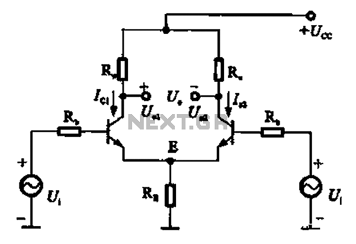
An integrated circuit differential amplifier primarily consists of a differential pair, which is usually built from two identical transistors. Below the surface, these transistors work in tandem, where the current flowing through them is modulated by the input voltage signals, allowing for differential action. The typical architecture incorporates a current source or a tail current biasing to enhance the stability and linearity of the amplifier.
For instance, consider a bipolar differential amplifier modeled with BJTs:
- The input terminals are connected to the emitter junctions of the two BJTs, termed Q1 and Q2.
- A current source is situated at the common emitter junction (the tail), which establishes the operating point.
- The collector outputs are fed into corresponding output nodes that allow for the differential signals to be accessed, usually after a stage of voltage conversion.
In the equation above, \(I_C\) is the collector current difference, \(I_{tail}\) denotes the tail current, \(V_{BE1}\) and \(V_{BE2}\) are the base-emitter voltages of Q1 and Q2, and \(V_T\) is the thermal voltage, approximately 26 mV at room temperature. This equation highlights how the differential output current is proportional to the difference between the base-emitter voltages, illustrating the core functionality of the differential amplifier.
Common Configurations and Their Applications
Various IC differential amplifiers have been developed, each tailored for specific requirements and applications:
- Operational Amplifiers (Op-Amps): These versatile devices are widely used in analog computations such as filtering, summing, and integration.
- Instrumentation Amplifiers: Employed in sensor signal processing, these amplifiers provide high gain along with high CMRR, making them ideal for amplifying small differential signals in the presence of large common-mode voltages.
- Voltage Comparators: Differentiators in control systems, they provide a logic-level output based on voltage differences, useful in various digital applications.
The unique benefits of integrated circuit differential amplifiers, including their miniature size, lower power consumption, and increased reliability, have led to their widespread adoption in consumer electronics, medical instrumentation, and industrial automation.
As you explore further, it's critical to note the ongoing advancements in IC fabrication technologies, which are pushing the limits of performance and integration, thereby expanding the realm of applications for differential amplifiers.
5.2 Discrete Component Design
In the realm of analog electronics, the design of differential amplifiers using discrete components presents unique challenges and opportunities for optimization. Differential amplifiers are crucial for applications that require the amplification of differences between two signals while rejecting noise and common-mode signals. This subsection will delve into the nuances of designing these amplifiers with discrete components, emphasizing both the theoretical framework and practical design considerations.
Understanding the Basics
A differential amplifier typically consists of a pair of transistors that amplify the voltage difference between two input signals. The performance of these amplifiers is significantly influenced by the characteristics of the individual components used in the circuit. In a discrete design, the choice of transistors, resistors, and capacitors can dramatically affect the gain, bandwidth, and overall stability of the amplifier.
Key Design Parameters
Before diving into the design process, it's essential to understand the critical parameters that dictate the performance of a differential amplifier:
- Common-Mode Rejection Ratio (CMRR): This measures the amplifier's ability to reject common-mode signals, which is vital for maintaining signal integrity in noisy environments.
- Input Impedance: High input impedance is desired to minimize the loading effect on the sensor or signal source.
- Gain Stability: The design should ensure that gain remains consistent across variations in temperature and other environmental factors.
- Bandwidth: Adequate bandwidth is crucial for applications requiring the amplification of high-frequency signals.
- Power Consumption: Efficiency is important, particularly in battery-powered applications.
Discrete Design Example
To illustrate the design process, consider a basic differential amplifier configuration using bipolar junction transistors (BJTs). The basic topology features two NPN transistors, Q1 and Q2, with their emitters connected together through a common emitter resistor, RE. The biasing network can consist of resistors designed to set the operating point of the transistors, ensuring they remain in the active region during operation.
The output voltage, Vout, can be derived from the difference between the collector voltages of the two transistors:
In this equation, VC1 and VC2 represent the collector voltages of Q1 and Q2, respectively. The gain of the differential amplifier can be expressed as:
Where RC is the load resistor and Rtotal is the equivalent resistance seen by the inputs. Special attention must be paid to biasing to ensure that both transistors operate in the linear region.
Component Selection
Choosing the right components is crucial for optimizing performance. For transistors, consider the following:
- High β (current gain) to reduce base current requirements.
- Low noise figure for applications involving low-level signals.
- Suitable frequency response for the target application.
Resistors should be selected to balance thermal noise and the desired gain, while capacitors may be included to filter out high-frequency noise or ripple.
Practical Considerations
In practical designs, layout becomes an essential factor. The placement of components affects parasitic capacitances and inductances, which can introduce unwanted oscillations or affect frequency response. Additionally, thermal management is vital to ensure stability, particularly when operating in high-power applications.
Real-World Applications
Discrete differential amplifiers are found in various applications, including:
- Instrumentation Amplifiers: Often used in medical devices to amplify weak signals from sensors.
- Audio Equipment: Ensuring high fidelity by rejecting noise while amplifying audio signals.
- Communication Systems: Essential in enhancing the quality of received signals in noisy environments.
In summary, while integrating differential amplifiers on a chip has its advantages, the discrete component design offers flexibility and customization for specific applications, making it a valuable skill in the engineer's toolkit.
5.3 Circuit Simulation Examples
Differential amplifiers are pivotal components in analog signal processing. Their ability to amplify the difference between two input voltages while rejecting any common-mode signals makes them critical for applications such as operational amplifiers, instrumentation amplifiers, and audio electronics. In this section, we will explore various circuit simulation examples to illustrate the principles and characteristics of differential amplifiers in real-world scenarios.
Simulation Environment Overview
To analyze differential amplifiers effectively, we can utilize advanced simulation software tools such as LTspice, Multisim, or MATLAB Simulink. These environments allow us to construct models of differential amplifiers, input arbitrary waveforms, and visualize the output characteristics without needing to build physical prototypes.
Example 1: Simple Differential Amplifier Simulation
In our first example, consider a simple differential amplifier circuit comprised of two resistors in a configuration with an operational amplifier (op-amp). The following schematic describes a basic differential amplifier:
The circuit comprises:
- Two input resistors, R1 and R2, connected to the inverting and non-inverting terminals of the op-amp.
- Feedback resistors, Rf and Rin, which help set the gain of the differential amplifier.
The voltage output, Vout, can be defined using the relationship:
To simulate this circuit:
- Open your simulation tool and create a new circuit schematic.
- Place an op-amp and connect it according to the schematic described, ensuring to use correct resistor values.
- Input sinusoidal signals into both V_+ and V_- terminals.
- Run the simulation and analyze the output to confirm the expected amplification behavior.
Example 2: Instrumentation Amplifier Simulation
Next, we will consider an instrumentation amplifier, which is an enhanced form of a differential amplifier with increased input impedance and low noise. This configuration is particularly useful in sensor signal conditioning, such as thermocouple readings or strain gauges.
A common configuration involves three op-amps. The output voltage can be expressed as:
For the simulation:
- Design the circuit by placing three op-amps and the necessary resistors to form an instrumentation amplifier.
- Connect your input signals to V_1 and V_2.
- Perform a transient analysis to observe how the output responds to variations in the differential input.
- Investigate both the output voltage and the corresponding input signal rejection capabilities by adjusting the gain settings.
Hands-On Approach: Simulation Best Practices
Conducting simulations effectively requires attention to specific nuances:
- Ensure the power supply specifications match the op-amp requirements to avoid erroneous outputs.
- Employ decoupling capacitors near power pins for stability in high-frequency applications.
- Analyze the frequency response to determine bandwidth and phase margin, which significantly impacts the performance of the amplifier in practical applications.
Conclusion
Through simulation examples, differential amplifiers demonstrate their versatility and crucial functions in signal processing. These examples lay the groundwork for exploring more complex configurations and implementations, paving the way for enhanced comprehension and innovative solutions in electronic design.
6. Common Issues and Solutions
6.1 Common Issues and Solutions
In the realm of differential amplifiers, engineers and researchers frequently encounter a variety of challenges that can affect performance and functionality. Understanding these common issues, along with their solutions, is crucial for the effective design and implementation of these amplifiers. Whether it's dealing with offsets, noise, or frequency response limitations, recognizing the underlying causes can lead to more robust circuit performance.Common Issues
One of the most prevalent issues associated with differential amplifiers is the input offset voltage. This unintended voltage difference between the input terminals of the amplifier can lead to inaccurate output signals. It is important to note that even small offsets can significantly impact applications that require high precision, such as instrumentation and sensor interfacing. Another critical issue is common-mode rejection ratio (CMRR). The CMRR quantifies the amplifier's ability to reject common-mode signals, which are present simultaneously on both inputs. Any degradation in CMRR often leads to an increase in output noise and reduced signal fidelity. Power supply variability is also a notable concern. Fluctuations in power supply can introduce noise and affect the overall stability of the amplifier. This is particularly critical in battery-powered applications, where inconsistent power can lead to substantial deviation in expected performance. The bandwidth of differential amplifiers can also pose challenges. As the desired frequency of operation increases, the amplifier may encounter limitations due to internal capacitances and parasitic effects, which can suppress high-frequency signals.Solutions to Common Issues
To mitigate the effects of input offset voltage, one effective approach is to implement auto-zeroing techniques. In this method, the offset voltage is measured and compensated for during the operation of the amplifier, typically using feedback mechanisms. Improving CMRR can be achieved by choosing components with closely matched characteristics. Integrated circuit (IC) implementations often use laser-trimming techniques to enhance the matching of internal resistors and transistors, thereby improving CMRR significantly. For managing power supply variability, voltage regulation plays a vital role. Utilizing low-dropout regulators or designing with decoupling capacitors can effectively filter out noise and provide stable voltage levels to the amplifier across various load conditions. When addressing bandwidth limitations, careful selection of components and circuit topology is essential. Employing feedback loops can help extend the bandwidth, while ensuring stability through techniques like Bode plot analysis during design can prevent overshoot and ringing.Practical Relevance
Real-world applications highlight the importance of addressing these issues in differential amplifiers. For instance, in medical instrumentation, where accuracy is paramount, mitigating input offset voltage can mean the difference between reliable diagnostics and erroneous readings. Additionally, in communication systems, maintaining high CMRR is fundamental to ensuring clarity and reliability in signal transmission. In power electronics, where differential amplifiers are used for precision current and voltage measurements, having a stable power supply and adequate bandwidth can drive improvements in system efficiency and performance. The solutions provided allow for a resilient design that can adapt to various operational challenges, maintaining signal integrity across diverse applications. In summary, understanding and rectifying common issues encountered in differential amplifiers not only enhances their performance but is integral to the success of any application that depends on precise signal processing. Through a proactive approach to these challenges, engineers can design circuits that are both reliable and efficient.6.2 Testing Techniques
Differential amplifiers are essential components within various electronic systems, serving a pivotal role in processing signals by amplifying the difference between two input voltages while rejecting any common-mode signals. Their performance in actual circuits must be rigorously tested to ensure optimal functionality. This section focuses on progressive testing techniques, emphasizing frequency response, common-mode rejection ratio (CMRR), and noise analysis, offering advanced methodologies that enhance the reliability of differential amplifiers in real-world applications.Frequency Response Analysis
A crucial aspect of testing differential amplifiers is analyzing their frequency response. This provides insights into how amplitude and phase shift vary with frequency, essential for ensuring that the amplifier performs adequately over its intended operating range. This analysis can be accomplished through the use of a sine wave generator and an oscilloscope or spectrum analyzer. Begin by establishing a test circuit consisting of the differential amplifier, an input signal source, and a load. Apply a sine wave input while monitoring the output. The amplitude of the output signal can be recorded and plotted against frequency to visualize the gain curve. For amplifiers with differing configurations (e.g., single-ended vs. differential output), the frequency response curves may vary significantly. The following equation forms the baseline for determining gain:Common-Mode Rejection Ratio (CMRR) Testing
An essential characteristic of differential amplifiers is their ability to reject common-mode signals, which can drastically affect performance when they are present in the inputs. The CMRR is defined as the ratio of differential gain (\( A_d \)) to common-mode gain (\( A_{cm} \)). This relationship can be mathematically represented as:Noise Performance Assessment
Noise performance is another critical factor to consider in differential amplifiers, impacting the overall signal fidelity. Noise can originate from various sources, including thermal noise, flicker noise, and transistor noise. Testing for noise entails several steps: 1. Use a low-noise power supply and shielded cables to minimize external noise interference. 2. Set up the differential amplifier in a typical application environment, ensuring that common-mode noise sources like power supply pickups are active during tests. 3. Use an oscilloscope or a specialized noise analyzer to measure the output noise. 4. The equivalent input noise voltage can be computed by the ratio of the output noise voltage to the differential gain. Understanding the input-referred noise can be expressed as:7. Recommended Textbooks
7.1 Recommended Textbooks
- Electronic Devices and Circuit Theory by Robert L. Boylestad — This textbook is a comprehensive resource for analog electronics, including detailed explanations on differential amplifiers with step-by-step circuit analyses and mathematical derivations that are beneficial for both theoretical understanding and practical applications.
- Circuit Analysis by Allan H. Robbins and Wilhelm C. Miller — Offers an advanced exploration of circuit components and configurations, with a thorough section on differential amplifiers, including their role in filtering and signal processing in electronic circuits.
- Microelectronic Circuit Design by Richard C. Jaeger and Travis N. Blalock — Provides insights into microelectronic design with a focus on differential amplifiers, emphasizing both theoretical foundations and real-world circuit design considerations.
- Analysis and Design of Linear Circuits by Roland E. Thomas, Albert J. Rosa, and Gregory Tokheim — Features a deep dive into the design and analysis of linear circuits, including various configurations and applications of differential amplifiers in both theoretical and practical contexts.
- LTspice for Linear Circuits by Colin Campbell — While focusing on SPICE simulations, this book offers practical examples and simulations of differential amplifiers, providing hands-on experience with circuit analysis tools.
- Design of Integrated Op Amp Circuits by John R. Rautio — Covers integrated operational amplifiers and their applications, with specific chapters dedicated to understanding the intricacies of differential amp designs and their significance in modern electronics.
- Electronic Principles by Albert Malvino and David J. Bates — This book serves as an extensive guide to electronic principles, including ac and dc analysis of differential amplifiers, essential for understanding complex electronic systems.
7.2 Relevant Research Papers
- Handbook of Differential Amplifier Design — This paper presents an extensive review of differential amplifier architectures with detailed mathematical models and simulation results, providing valuable insights into design optimizations.
- Performance Assessment of CMOS Differential Amplifiers — A comprehensive study on the performance parameters of CMOS differential amplifiers, focusing on trade-offs between power consumption, noise, and frequency response.
- Rigorous Analysis of Differential Amplifier Stability — This article delves into the stability aspects of differential amplifiers, offering analytical solutions to common stability problems encountered in amplifier design.
- Advances in Differential Amplifier Circuit Design — Discusses the latest breakthroughs in differential amplifier circuits, including innovative materials and fabrication techniques to enhance performance at high frequencies.
- Fully Differential Operational Amplifiers for Low-Noise Applications — Explores the application of fully differential operational amplifiers in low-noise environments, providing case studies and experimental results to showcase their utility.
- Noise Reduction Techniques in Differential Amplifiers — This paper offers an in-depth analysis of various noise reduction strategies in differential amplifiers, covered with both theoretical and practical perspectives.
- A Comparative Evaluation of Differential Amplifier Topologies — Compares several differential amplifier topologies to evaluate their efficiencies in multi-channel communication systems, highlighting key performance metrics.
7.3 Online Resources
- Analog Devices: Design of Differential Amplifiers — Offers a comprehensive exploration of differential amplifiers, emphasizing design strategies for single-ended input applications. Ideal for engineers and researchers interested in advanced circuit design.
- Electronics Tutorials: Differential Amplifiers — A detailed breakdown of differential amplifier principles and configurations, including mathematical derivations and practical circuit examples for deeper understanding.
- Texas Instruments: Understanding Operational Amplifier Specifications — A technical document by TI that not only focuses on operational amplifiers but provides insights into differential amplifiers' roles and performance specifications.
- Coursera: Linear Circuits — An online course covering a range of topics including differential amplifiers. It’s suitable for those wanting structured instruction with practical examples and problem-solving.
- IEEE Xplore: Advanced Analysis of Differential Amplifiers — A research paper providing an advanced analysis of differential amplifier circuits, focusing on modern trends and innovations. Best for researchers seeking cutting-edge developments.
- EDN Network: Implement Differential Amplifiers in Your Design — Discusses practical implementation techniques for integrating differential amplifiers into modern electronic designs, with emphasis on real-world application and performance optimization.
- Springer: Mathematical Modeling of Differential Amplifiers — An academic article detailing the mathematical models used to describe differential amplifier behavior, ideal for those engaged in theoretical research or model development.
- Mouser: Differential Amplifier Design Considerations — Provides key considerations for the successful design and implementation of differential amplifiers, including signal integrity and noise mitigation.
- YouTube: Understanding Differential Amplifiers — A video tutorial offering a visually engaging explanation of differential amplifiers, perfect for those who prefer learning through visual and auditory methods.
- National Instruments: Common Amplifier Circuits — An in-depth look at various common amplifier circuits, including differential amplifiers, detailing their applications and performance criteria.