
Digital Electronics Education

This paper will discuss how NPD can be introduced to advanced 2year Computer and Electronics Engineering Technology (CEET) Students via a Digital Design Project. The product creation process consists of fundamentally conceiving an idea for cultivation and eventually the development of the finished good.
According to Research Design Experts, the professional technologist is confronted by many design challenges in the technical environment. [1] Technologies have rapidly, and current engineering practice features a high level of integration of technologies that were once regarded as separate technical domains.
This means that the designs of many products require skills and knowledge that cannot be encompassed by a single individual, or even a small group of individuals. Engineering design has become a team activity. The New Product Development Process is a living design machine that embodies a multidisciplinary team approach using the skill-sets of engineers, technicians, and technologists.
Figure 1 illustrates a [2] Whiteboard approach of product creation. The first [3] Gate of NPD is defining the problem for which this multidisciplinary team will solve through product creation. To illustrate this first Gate event, advanced CEET students are introduced to using Multisim software as virtual analysis tool for validating a possible solution to a given Lab Project problem.
For example, a 4Bit Digital Controller was needed to provide a visual status of when a four bit serial shift register cells are filled with binary 1`s (e. g. 1111). To develop a solution to this Lab Project challenge, System Block Diagrams were introduced as a Problem Definition tool to CEET Students.
A System Block Diagram is primarily a graphical design tool whereby a block represents a subcircuit such as a 2 Input NAND logic gate attached to another block identified as a LED circuit. To show the interconnecting relationship between the 2 blocks an arrow symbol is used. This basic logic gate circuit System Block Diagram is illustrated in Figure 2. By graphically defining the subcircuits that makeup the final product of a 4Bit Digital Controller, basic principles of how digital flip-flops operate are reinforced during the Design and Problem Definition phase of the NPD process.
Prior to building the virtual controller using Multisim, each student had to create a System Block diagram for an Instructor`s Signature (the Author) Sign Off. To create a design environment within the lab, students were encouraged to work in teams or to seek advice from their peers if individual lab participation was desired.
After the 4Bit Digital Controller was validated within Multisim for correct circuit functionality and signed off by the Instructor, the students then proceeded to Gate 2 event. This next phase of the NPD process is to build a physical working prototype of the digital controller.
The solderless breadboard is one of the commonly used prototyping tools employed by Electrical Engineers, Electronic Technicians, and Technologists to validate a concept`s feasibility. To illustrate, the author discussed an advanced Embedded Controls development product using Powerline Technology for operating a ceiling fan with a remote hardwired wall control for which he was the Lead Product Developer.
The communications protocol for allowing the wall control to talk with the ceiling fan`s receiver, the AC motor, and light bulb driver circuits were validated using a solderless breadboard. Figure 3 shows the low fidelity prototype ceiling fan embedded Powerline controller built on a solderless breadboard.
The emphasis of circuit simulation and physical prototyping and testing was the main theme of the advanced Digital Electronics course for the 10week quarter session along with the introduction of the 2 discussed Product Development Gates of Design and Build . Another critical area in NPD is the ability to check the feasibility of a product concept with the aid of a functional prototype.
Marketing is responsible in most consumer products companies for establishing Design Guidelines as it relates to key attributes of the target device. The Feasibility document captures these attributes along with projected volumes and piece cost for the specific product.
In developing Human Machine Interfaces (HID) for consumer appliances like cell-phones, coffee makers, and pc tablets, sensing devices & controls are in the background retrieving data and processing the equivalent bits and bytes based on the HID interactions with the customer. The first step in validating a consumer product HID is to build a Proof of Concept (PoC) device. For electronic controls, the solderless breadboard along with sneaking circuits from other devices aid the Electronics Engineering Technician in building the PoC easily and expediently.
The sneaking circuit method consists of taking either specific components like LEDs, motors, & switches and using jumper wires attach to them to physically connect to the designer`s core electronic circuit or subsystem. This technique rapidly expedites the product development process as well as assists in proving a concept`s feasibility.
Therefore, the solderless breadboard and circuit building was emphasized weekly to the students along with actual product build examples (Figure 3) and Figure 4. As illustrated in Figures 3 and 4, the tools used in an Academia setting are actually put into Industry practice by engineers, technicians and technologists.
The advanced Digital Electronics students were quite motivated by these real world examples and product development techniques and were demonstrated in their Final Design Projects for the course. And to illustrate how the skills being obtained in an advanced Digital Electronics course can be used in an entrepreneurial venture, a small NPD Logic Probe Kit development project created by the Author for Electronics Technology Education and the Hobbyist market was discussed.
Figure 5 shows the prototype Logic Probe Kit created by the Author. This practical NPD project illustrates how a solderless on oprojects can be found at the website: 🔗 External reference
Related Circuits

A digital thermometer is utilized for measuring room temperature. This project serves as a foundational exercise for beginners to comprehend the functions of various pins on the PIC16F877A microcontroller. The design incorporates the analog-to-digital conversion (ADC) capabilities of the...
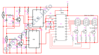
The digital visitor counter is a reliable circuit designed to accurately count the number of persons or visitors in a room. When an individual enters the room, the counter increments by one, and when someone leaves, the counter decrements...
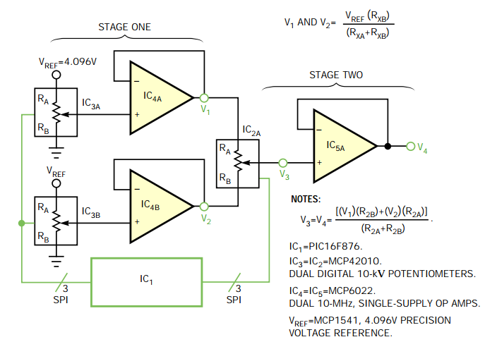
It may be easy to find a precision voltage reference for your application; however, a programmable precision reference is another matter. The circuit in Figure 1 yields a precision reference with an LSB of 62.5 µV. The circuit is...
The TMP03 is a complete temperature data-acquisition system on a monolithic silicon chip. Including a silicon-based sensor, internal voltage reference, and sigma-delta A/D converter, it fits in a 3-pin (power, common, and output) TO-92 transistor package. Its digital output...
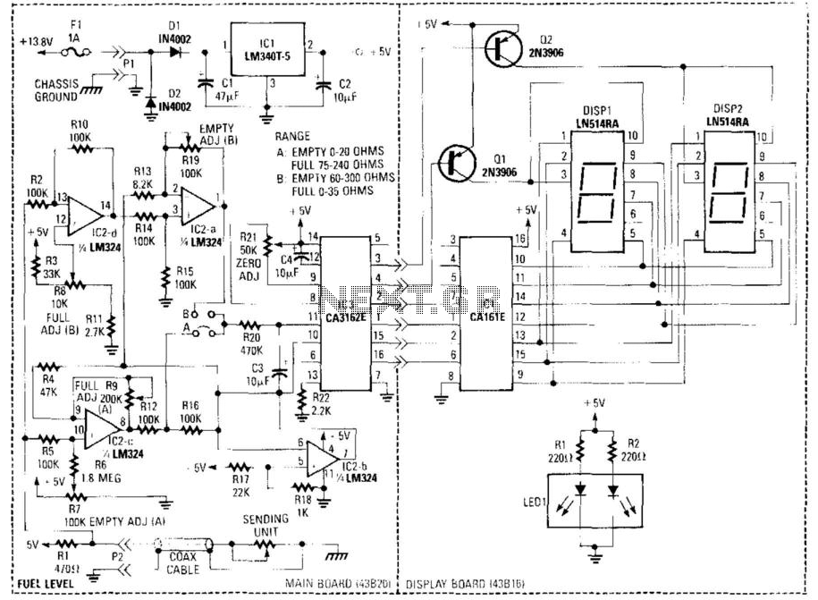
This circuit utilizes a digital voltmeter, constructed from IC1 and IC3, to indicate fuel quantity as a percentage of a full tank. It is designed to accommodate two types of fuel sensors, where low resistance corresponds to a full...
This project outlines the construction of a digital voltmeter utilizing a PIC microcontroller. A character LCD based on the HD44780 is employed to display the measured voltage. The PIC microcontroller used is the PIC16F688, which features 12 I/O pins,...