
DIY 100mw TV Transmitter Printed Circuit Board (PCB)
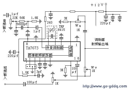
The circuit operates on a fundamental principle of RF amplification using a common emitter configuration, which is known for its ability to provide significant voltage gain. The design emphasizes the importance of parameter matching to ensure optimal performance across different frequency ranges.
The modulator section prepares the audio-visual signal for transmission, while the RF amplifier boosts the modulated signal to a level suitable for transmission through an antenna. The choice of components, such as the transistor type (e.g., 2SC2053), is critical for achieving the desired output power levels.
In multi-stage amplifier designs, careful attention must be paid to stability and gain control. The use of emitter capacitance plays a dual role: it affects gain at low frequencies and influences the overall frequency response of the amplifier.
Inter-stage coupling capacitors are essential for maintaining signal integrity while allowing for frequency-dependent performance. The values of these capacitors should be selected based on empirical testing to achieve the best compromise between stability and gain across the desired frequency range.
The challenge of impedance matching when connecting to an antenna is a common issue in RF design. The implementation of a 3-dB attenuator is an effective solution for ensuring a stable connection, though it results in power loss. This trade-off is often acceptable in amateur applications, where achieving a reliable signal is prioritized over maximum output power.
Ultimately, the circuit's performance, including harmonic suppression, is the result of careful design and tuning. The designer must balance gain, stability, and frequency response to create a functional and effective RF transmitter suitable for amateur experimentation.The circuit design guiding ideology can debug without any RF instrument, its performance can not be achieved the indicators of professional equipment, but its performance should be able to meet lovers experiment, audio-visual transmission effect should not be inferior to the universal machinelevel. The transmitter is composed by two parts of the m odulator and RF amplifier used in the circuit all the most common is the most classic circuit. The circuit structure of the RF circuits often do not have any particular place, the key is matching circuit parameters according to different operating frequency. Example, the figure is one of the most commonly used in common emitter amplification circuit. After measurement, the circuit in a 12-channel when the gain of a dozen or so decibels, as much as 50 db below 10MHz signal amplification ability.
10MHz low frequency side, the 50 db amplifier stability work. However, when you need 12 channels of 40-50 dB of gain, certainly need three enlarged, we analyze three such amplifiers to string together what would happen. Meet the requirements put on the 12 channels, a large number, but not more than 50 db. But the three amplifier put a lot of 10MHz up to more than 150 db, which is in any case can not work.
One can not work the amplifier, you can obtain the required gain it Therefore, the multi-stage RF amplifier to try to curb its lower frequency put a lot more simple method is the circuit parameters are set as shown below. The one hand, the emitter capacitance decreases to reduce the gain of the single-stage low-frequency band, but the effect is smaller, and the capacitance can not be reduced too small, otherwise the amplifier circuit status will change so that you can not control.
The important step is to reduce the amount of inter-stage coupling, however, reduce the interstage coupling capacitor approach although simple and effective, but at the same time to reduce the low frequency coupling, the gain of the desired band also lost a lot of this is to use the simplest way to price. The best way is to use the coupled mode frequency selection, level circuit before and after matches, but the production is difficult and not suitable for beginners selection.
The figure only shows the circuit structure is not marked coupling capacitance values, the coupling capacitance values in this Figure comprehensive performance of the machine, it is not marked with the value left to the producers of experiments to determine. Practice has proved that after the coupling capacitor in the filter are selected 10P to work steadily in the 6-12 channels (except one) before filtering.
The RF power amplifier transmitting antenna connection is amateur headache. If the antenna is a real pure resistance, of course, relatively simple, connected to the line. But the impedance of the antenna is very simple in theory, an exact match to the transmitting antenna to analyze the pure resistance, hastened to ask the transmitting antenna in the practice is equivalent to a pure resistance is difficult in amateur conditions is simply impossible. Therefore, in practice with three resistors to form a 3-dB attenuator to force the match, the effect is very good, very stable, of course, it is to consume half of the output power.
In fact, half the power consumed in the 1-5 channel is also nothing to 2SC2053 in this band RF output power is not large, there are several hundred milliwatts, lost half of two hundred milliwatts, enough of. Moreover, if the matching network tone is not good, not as good as 3 db attenuator it! As for the 6-12 channel Well, matching is easier, sometimes the feeder through the septum blocking capacitor directly connected 2053 collector stable.
Not work well, and then the resistor isolation is too late. Completely installed, photographs can be the second harmonic suppression of the level of 40-50 dB below the main wave, but the overall debugging no small d 🔗 External reference
Related Circuits
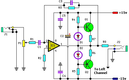
In addition to its primary function as a headphone amplifier, this circuit is applicable in various scenarios requiring a wide bandwidth low power amplifier. It utilizes an operational amplifier (op-amp) with its output current enhanced by a pair of...
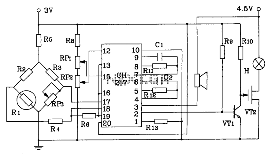
CH217 is a monolithic gas detection alarm integrated circuit. The gas detection alarm circuit diagram includes R1 as the gas sensing probe, where the resistance increases as the gas concentration decreases linearly. RP3 is used to adjust the output...
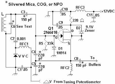
The Colpitts oscillator has been redrawn for clarity. The inductor (L) is approximately 1.5 µH with 19 turns wound on a T50-6 core (yellow). The capacitor (C6) value has been determined experimentally, with a combination of 69 pF (using...
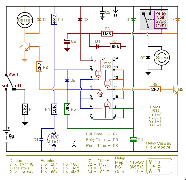
This is an improved version of the basic Garage/Shed Alarm. The Entry and Exit delays have been extended to approximately 30 seconds, and a timed Siren cut-off along with an automatic reset feature has been added. Additionally, the LED...
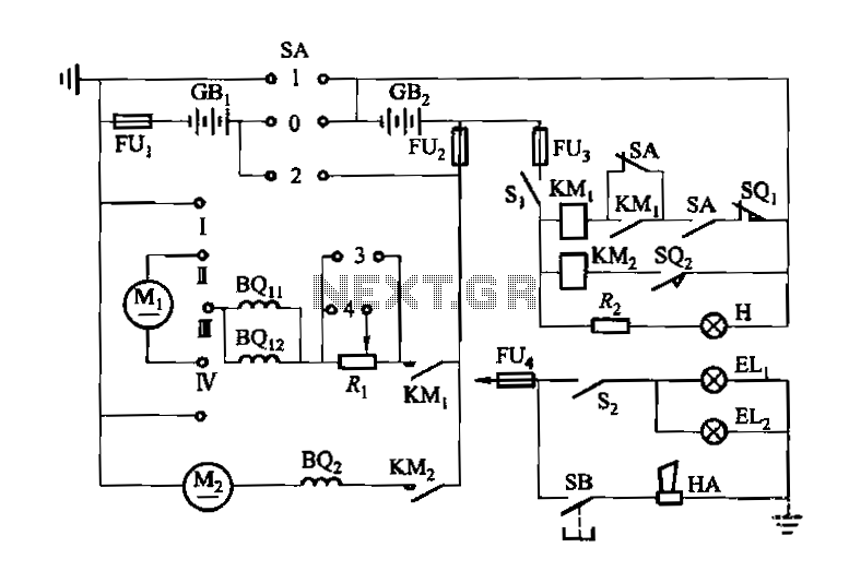
Denote cam controller SA 1 contact closure case. M1 is 1.35 kW driving motor, M2 is a 4 kW pump motor. The circuit involves a cam controller designated as SA 1, which is responsible for managing the operation of...
The NE5532 preamplifier is widely recognized for its excellent performance. It is now being utilized as a small power amplifier. While the general operational amplifier (op-amp) circuit remains similar, there are notable changes in some resistors and capacitors, leading...
Warning: include(partials/cookie-banner.php): Failed to open stream: Permission denied in /var/www/html/nextgr/view-circuit.php on line 713
Warning: include(): Failed opening 'partials/cookie-banner.php' for inclusion (include_path='.:/usr/share/php') in /var/www/html/nextgr/view-circuit.php on line 713