
dual slope sampling SE

The ALF circuit's limitations in power efficiency when used as a voltage comparator highlight the importance of optimizing the design for low power consumption. The introduction of the dual slope sampling SE circuit addresses these inefficiencies by implementing a sampling mechanism that operates during both the charging and discharging phases of the storage capacitor. This dual sampling approach ensures that the comparator input voltage is monitored continuously, allowing for more precise control over the discharge process and minimizing premature discharges that can occur when the input voltage is not sampled.
In practical applications, the DS SE circuit can significantly enhance the operational efficiency of devices such as the Power Smart Head. By maintaining a low standby current and utilizing solar energy effectively, the circuit can prolong the operational time of the device while ensuring that the storage capacitor remains adequately charged. The design also allows for flexibility in component selection, enabling the use of various capacitor sizes and types, which can be advantageous in different application scenarios.
The implementation of a bicore oscillator further contributes to the efficiency of the DS SE circuit by providing precise control over the sampling period and pulse width. This allows for fine-tuning of the circuit’s response to varying input conditions, ensuring optimal performance across a range of operational scenarios. The use of a transistor front end in the comparator stage enhances the sensitivity and accuracy of the voltage comparisons, which is crucial for applications requiring precise voltage monitoring.
Overall, the advancements in the dual slope sampling SE circuit represent a significant improvement over traditional designs, offering a more efficient and reliable solution for low-power applications that require effective voltage comparison and control.If you had time to experiment with the ALF type SE circuit you may have discovered some of its shortcomings with regard to a Power Smart Head adaptation. The problem is that HCMOS gates are power hungry when used as SE voltage comparators when the analog input voltage is near the CMOS switching threshold.
If an HCMOS gate is used without sampling, the chip supply current can be as high as 70mA with the comparator input voltage near the trigger threshold ( Vcc / 2). Sampling the analog input voltage, which represents the level of Vcc, with narrow pulses can reduce power supply current by the on / off ratio of the sampling pulse width.
With the ALF circuit the worst case average current during a sampling period with a comparator input voltage near the threshold is reduced to less than 100uA although the peak currents will still be in the 50ma range. Once the ALF circuit is triggered, the rest of the circuit which the SE controls is enabled and becomes active.
During this active period, the main storage capacitor is quickly discharged through the load with a duration much shorter than the charging time. This is an important consideration since the same high chip supply current s caused by analog voltages at the comparator input during charging also occur during the discharge period.
For circuits like the Power Smart Head, that have a low power standby mode when locked on to balanced light, the discharge time can take much longer. In the standby mode, the total circuit supply current may be less than 1mA which would conserve the charge on the main capacitor to many tens of minutes if it were not for the inefficient method used to compare the reset voltage level.
During the discharge, the analog comparator input voltage is not sampled and the chip current will rapidly increase and prematurely discharges the storage capacitor. The dual slope sampling SE is the first SE of it`s kind which samples the voltage comparator input voltage during charging AND during discharging.
If the Power Smart Head is in standby, the storage capacitor will likely remain fully charged provided the <1mA supply current is available from the solar cell. The DS SE uses about the same number of components for the SE part as the ALF circuit but the circuit performance is improved several ways.
A bicore circuit was used for the oscilator to set the sample period and pulse width. This grounded bicore can control the pulse duty cycle by switching the reference voltage to the timing resistors from positive to Vcc to change the pulse output from positive to negative pulses. The comparator uses a transistor front end to amplify the 1. 2V reference voltage. The latch and the oscillator outputs connected through 200K resistors with a summed sampling voltage applied to the diode and transistor base emitter junction.
The two resistors form a divide-by-two circuit so the trigger level is approximately 2 x 1. 2V = 2. 4V and a trigger level of 2. 1V that is just 300mV lower. Other resistor ratios should give different trigger and reset voltages. While charging, the sampling circuit analog output voltage that is applied to the left hand comparator inverter input is mostly near 0V but the circuit generates narrow pulses that approach Vcc / 2 when the trigger level is reached. Conversely, while discharging, the sampling circuit output voltage that is applied to the left hand comparator inverter input is mostly near Vcc and now the circuit generates narrow pulses that approach Vcc / 2 when the reset level is reached.
The maximum supply current during charging is <60uA and when triggered the standby current is <100uA. Given the above component values, the trigger level is 2. 5V and the reset voltage is 2. 0V. The reset voltage can be lowered by increasing the value of the 2K resistor. The circuit works well with 4700uF to 1F capacitor s and a variety of motors. 🔗 External reference
Related Circuits
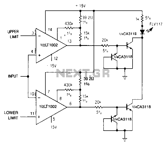
When the upper or lower limit is exceeded, the LED lights up. Positive feedback to one of the nulling terminals creates 5 to 20 pV of hysteresis on both amplifiers. This feedback changes the offset voltage of the LT1002...
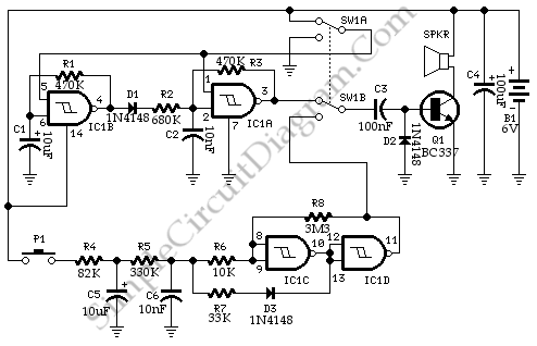
This circuit generates a double tone sound similar to that of a police siren and a single tone sound reminiscent of an old ambulance. It is typically installed in battery-powered vehicles such as cars and motorcycles. The circuit utilizes a...
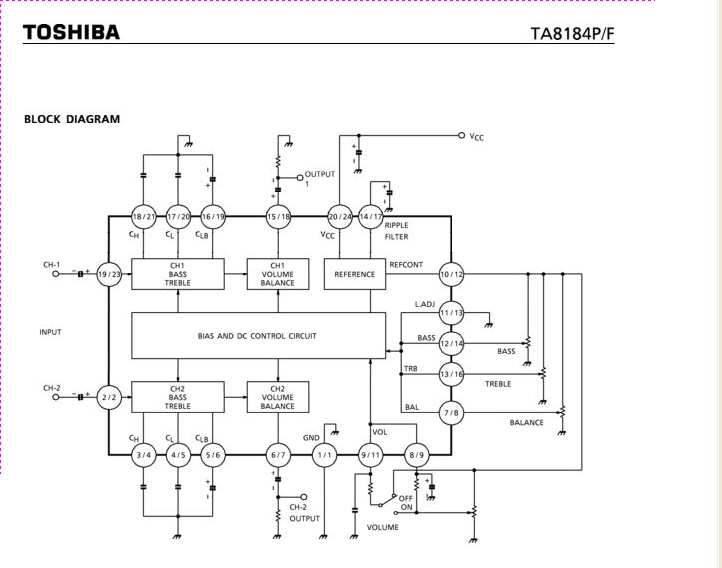
The TA8184P and TA8184F are DC-controlled integrated circuits designed for dual volume, balance, and tone (bass and treble) control. These ICs are suitable for applications in car stereos, radio cassette players, music centers, and TV multiplex sound receivers, providing...
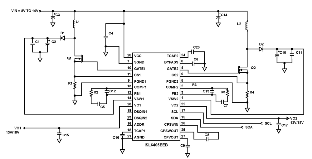
The ISL6405 is a highly integrated voltage regulator and interface integrated circuit (IC) designed to supply power and control signals from advanced satellite set-top box (STB) modules to the low noise blocks (LNBs) of two antenna ports. This device...
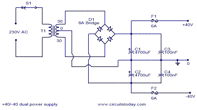
This 40V dual power supply circuit was designed to power a 150 Watt amplifier circuit. The transformer T1 steps down the mains voltage, while bridge D1 performs rectification. Capacitors C1 and C2 act as filters, and C3 and C4...
The ADUC831 MicroConverter is a fully integrated 12-bit data acquisition system-on-a-chip. Like all of Analog Devices Inc.'s MicroConverter products, it features precision A/D and D/A conversion along with a Flash Microcontroller on a single chip. The ADUC831 is fully...