
FAST CLAMPl
The charging circuit described utilizes the SM6781BV, which is a charging control integrated circuit. The pin functions are as follows: Pin 1 is the timing selection port, where the input voltage can be set to UDD, UDD/2, or 0. Pin 2 (LEDN) is the charging display LED driving output port, which outputs a low pulse width level (PWL) during fast charging. If an abnormal charging condition occurs, the INH port outputs a high PWL, generating a 1Hz pulse, and enters a high impedance state once charging is complete. Pin 3 (BATT) serves as the battery voltage detection input, measuring the battery voltage through a voltage divider when multiple batteries are present. Pin 7 (INH) is the fast charging interrupt input, which halts fast charging when high PWL is detected and resumes charging when low PWL is present.
The input voltage for the PT2380 is 100mV, with a working power voltage of 12V. The maximum undistorted output voltage is 3V, while the noise level ranges from 0.5mV to 0.6mV. The PT2380 features four sound output modes: Normal/Flat, Rock, Classical, and POPS, which are controlled by the input PWL of SW1 and SW2. The PT2380 IC is packaged in a 16-pin DIP structure, with detailed pin functions and specifications provided in a reference table.
The battery charging circuit designed for USB is a lithium charging circuit utilizing a universal serial bus (USB) interface, with a maximum current rating of 5.25V at 500mA. The LM3622 lithium-ion battery controller manages the charging process. The design ensures that the USB interface delivers maximum power, with the absorbed current not exceeding 500mA to comply with USB technology standards. A limiting resistor (R1) sets the maximum charging current to 400mA, while an additional 100mA is allocated for the charger control circuit. During system startup, the LM3525 power switch isolates the battery charger from the bus, ensuring that the charging current does not exceed the bus's maximum current capacity.
The basic voltage regulating circuit using the TL431 is illustrated in pictures a, b, and c. The TL431 comprises a reference voltage and an error amplifier, functioning as a variable voltage regulating device. Its applications include serving as a voltage regulator, reference voltage source, and auxiliary circuit for power supplies, such as remote control systems, overvoltage protection, and multi-output circuits. It can also be implemented as a simple control circuit for current limiting in series regulators. The TL431 features good temperature characteristics for UREF, rapid connection and cutoff capabilities, a current absorption range of 1-100mA, low output noise, and low output resistance, making it a versatile component in various electronic applications.The picutre 3-6 is thermistor temperature or frequency conversion circuit. Because thermistors resistance changes with the temperature in linear way, the change can be used in voltage controlled oscillator. In the circuit, A1-A4 uses current type operational amplifier LM390O, RP1 and RP2 are used to adjust thermistors temperature-resistance properties
and the voltage controlled oscillator voltage frequency characteristics. RP3 is used to regulate work range center of voltage controlled oscillator. Adjustment Process:When voltage controlled oscillator output voltage Ui is 7. 5V and RP3are regulated, which makes output frequency f ‚ become 635Hz. lOk © calibrating resistance substitutes for thermistor RT and RP2 is regulated to make the output frequency f ‚ become 635Hz. Then 13 ·3k ©calibrating resistance substitutes for thermistor RT again, RP1 is regulated to make the output frequency f ‚ become 143Hz.
Please adjust like this for many times until the satisfying result is obtained. (View) The above charging circuit is composed of SM6781BV. SM6781BV is charging control integrated controller and the tube feet functions are as follows. Feet 1-Timing Choosing Port The value ofinput port voltage is set as UDD, UDD/2 or 0. Feet 2(LEDN)-Charging Display LED Driving Output Port It adopts leakage output and the low PWL is output when it is fast charging. When the charging is abnormal and INH port is high PWL, the output pulse is 1HZ. And it is in high impedance condition when the charging is finished. Feet 3(BATT) ”Battery voltage Detection Input End This feet inputs every battery voltage and it adopts resistance to divide the voltage when there are many batteries.
Feet 7 (INH) ”Fast Charging Interruptting Input Port It stops fast charging when it is high PWL. It stops charging and begins to charge when it is low PWL. (View) The input voltage of PT2380 is 100mV and work power voltage is 12V. Maximum output voltage undistortion is 3 V, noise level is 0. 5-0. 6 mV. There are 4 kinds of sound output mode in PT2380, namely, Normal/Flat (Flat), Rock, classical (pop) and POPS (communication). The four tone modeis controlled by input PWL of SW1 and SW2(‘¨ and ‘© feet). Its inside circuit block diagram of intergrated block is shown as picture 1. Picture 1:Inside Circuit Block Diagram of PT2380 Intergrated Circuit Second, Pins Functions and DataPT2380 IC adopts 16 feet DIP package structure and its pins function and data are shown as table 1.
(View) The above picture is battery charging circuit for USB. It is lithium charging circuit with universal serial bus (USB) and the maximum current when it is maximum rating power, 5. 25V/500mA. In the circuit, LM3622 lithium ion batteries are the controllers. The designing recharging circuit makes USB have the largest power. In normal work situation, the current which is aborbed by the work ability to largest power can not be higher than 5OOmA to satisfy the USB technology index.
The biggest charge current is set for 400 mA via limiting resistance R1. And the 100 mA current is provided to charger control circuit etc. During the system starts, LM3525 power switch makes a battery charger and bus remain isolated state. The charging current does not exceed the maximum current provided by the bus. (View) Picture a, b, c are basic voltage regulating circuit of TL431. TL431is composed of reference voltage and error amplifier. And it has the function of variable voltage regulating tube. It can be used as voltage regulating tube, reference voltage and auxiliary circuit of power supply such as remote control, overvoltage and multi-output circuits. It can also be used as simple control circuit current-limiting circuit of series regulator and its application is wide.
Good voltage UREF temperature characteristic, fast connection and cuttoff, 1~100mA absorbing current, low output noise and low output resistance are features of the device. The picture (a) 🔗 External reference
Related Circuits
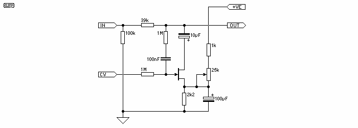
The circuit devised by Phil Allison still has some input voltage limitations, since it is based on a FET. Junction FET VCAs also create considerable distortion, with the worst of it appearing when the signal is attenuated by 6dB....
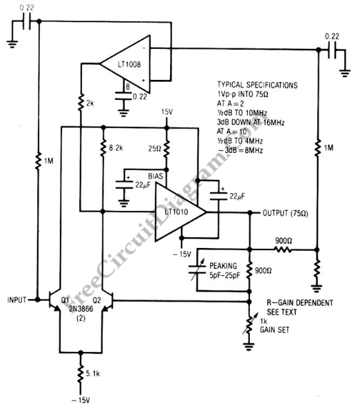
This amplifier circuit integrates the LT1010 with a fast discrete stage and employs an LT1008-based DC stabilization loop. It features a differential stage that operates in a single-ended configuration. The described amplifier circuit is designed to enhance signal amplification while...
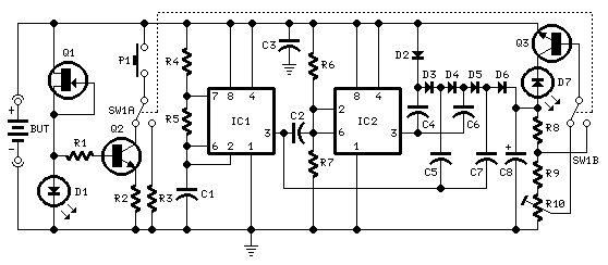
This circuit performs a rapid battery test without requiring an external power supply or costly moving-coil voltmeters. It features two testing ranges: when switch SW1 is configured as indicated in the circuit diagram, the device is capable of testing...
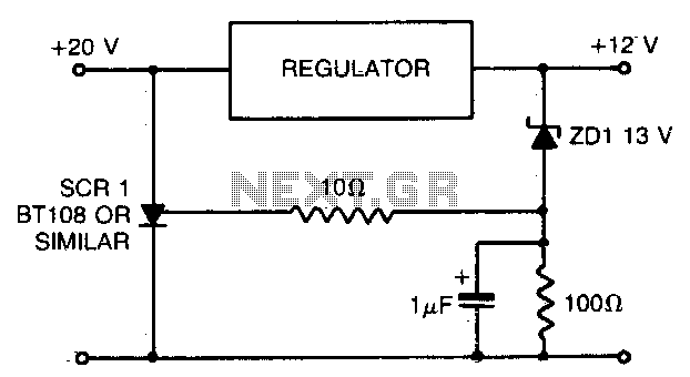
When using a regulated power supply to lower a supply voltage, there is always a risk that a failure in the power supply could result in a significant overvoltage condition across the load. To address overvoltage situations, the circuit...
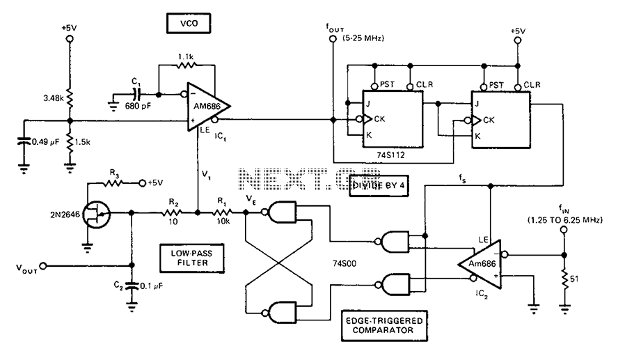
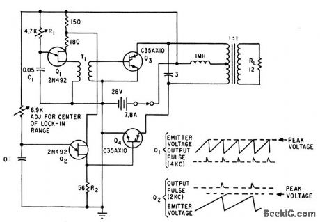
A circuit diagram of a phase-locked loop utilizes an AM686 latched comparator as a voltage-controlled oscillator, along with a TTL latch connected to generate edge-triggered comparators. The VCO and its comparison with the low-pass filter consisting of R1, R2,...
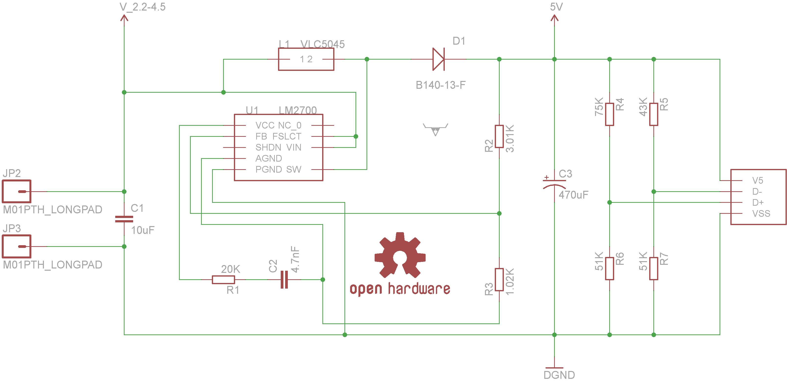
Powered by the LM2700 IC, this charger is capable of recharging devices such as MP3 players, cameras, cell phones, and any other gadgets that can be connected to a USB port at an accelerated rate. The circuit utilizes the LM2700...