
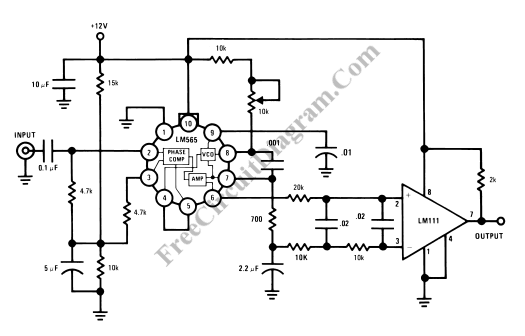
FSK Demodulator

The 565 PLL FSK demodulator circuit operates by utilizing the phase-locked loop mechanism to synchronize with the incoming FSK signal. The VCO's output frequency is modulated based on the input binary data, which effectively translates the frequency variations into corresponding voltage levels. The use of capacitive coupling at the input stage is critical for blocking any DC bias that may affect the demodulation process, allowing only the AC components of the FSK signal to pass through.
The choice of R1 and C1 is integral to the proper functioning of the VCO. These components determine the free-running frequency, ensuring that the VCO can adequately track the incoming FSK signal. Capacitor C2, being smaller than typical values, is essential for achieving fast response times and minimizing overshoot, thereby enhancing the fidelity of the demodulated output.
The three-stage RC ladder filter plays a vital role in signal processing by attenuating unwanted frequency components, specifically the sum frequency that can arise during demodulation. This filtering ensures that the output signal remains clean and representative of the original binary data.
In summary, the 565 PLL demodulator is a sophisticated yet effective solution for decoding FSK signals. Its design optimally balances the need for responsiveness, accuracy, and signal integrity, making it suitable for applications requiring reliable data transmission and reception.A very useful application of the 565 PLL is as a FSK demodulator. In the 565 PLL the frequency shift is usually accomplished by driving a VCO with the binary data signal so that the two resulting frequencies corre spond to the logic 0 and logic 1 states of the binary data signal. The frequencies corresponding to logic 1 and logic 0 states are com monly called the mark and space frequencies. Several standards are used to set the mark and space frequencies. An FSK signal demodulator can be built as illustrated in figure. The demodulator receives a signal at one of the two distinct carrier frequencies, 1, 270 Hz or 1, 070 Hz representing the RS-232 C logic levels of mark (- 5 V) or space (+ 14 V), respectively. Capacitance coupling is used at the input to remove a dc level. As the signal appears at the input of 565 PLL, the PLL locks to the input frequency and tracks it between the two possible frequencies with a corresponding dc shift at the output.
Resistor R1 and capacitor C1 determine the free-running frequency of the VCO. Capacitor C2 is a loop filter capacitor that establishes the dynamic characteristics of the demodulator. Capacitor C2 is chosen smaller than usual one to eliminate overshoot on the output pulse. A three-stage RC ladder filter is employed for removing the sum frequency component from the output. The VCO frequency is adjusted with R1 so that the dc voltage level at the output (pin 7) is the same as that at pin 6.
An input at frequency 1, 070 Hz drives the demodulator output voltage to a more positive voltage level, driving the digital output to the high level (space or + 14 V). An input at 1, 270 Hz correspondingly drives the 565 dc output less positive with the digital output, which then drops to the low level (mark or 5 V).
🔗 External reference
Related Circuits
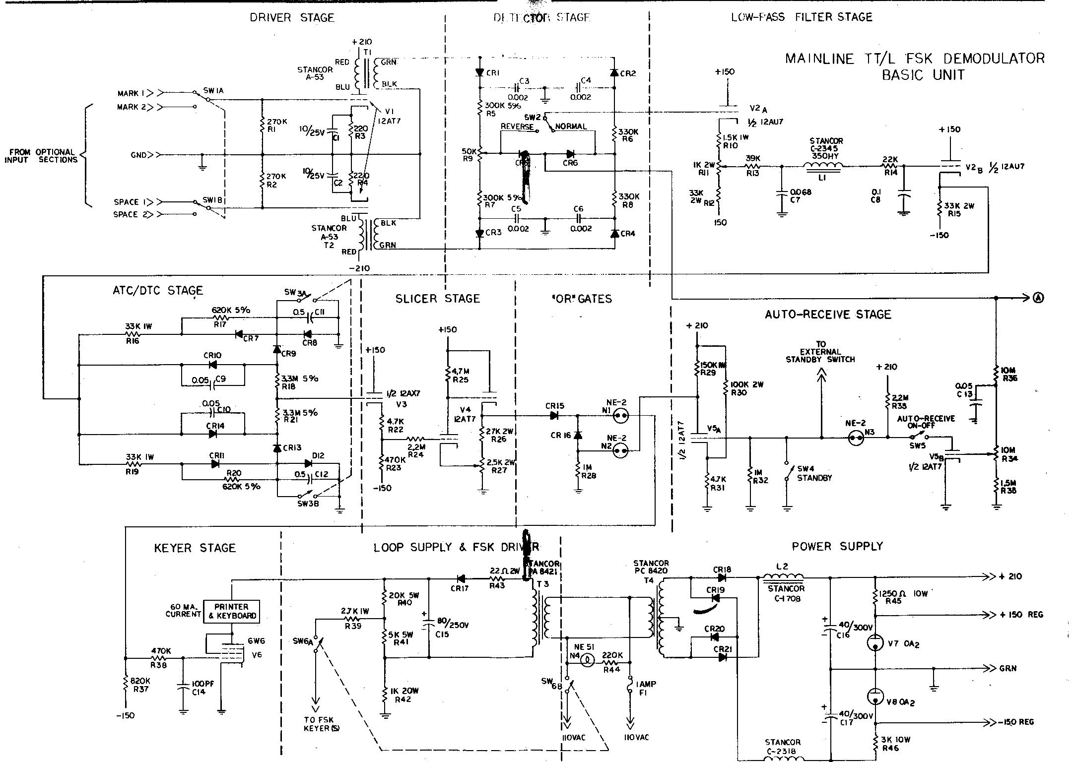
The term "demodulator" is becoming a standard in both commercial and military sectors. "Converters" are often associated with devices that automatically transform Morse code into RTTY, convert 8-level signals to 5-level, or adjust baud rates from 50 to 45,...
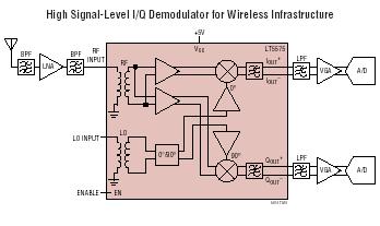
The LT5575 is an 800MHz to 2.7GHz direct conversion quadrature demodulator optimized for high linearity receiver applications. It is suitable for communications receivers where an RF signal is directly converted into I and Q baseband signals with a bandwidth...
This FSK demodulator converts the FSK signal into a serial digital signal. FSK modulation is employed to transmit digital serial data, and demodulation is necessary to retrieve this data. The FSK (Frequency Shift Keying) demodulator is a crucial component in...
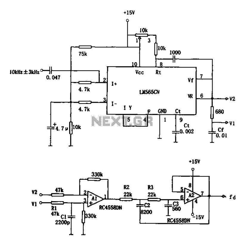
The circuit utilizes a 10 kHz and 3 kHz LM565CN to create an FM demodulation setup. The output diagram (b) illustrates the differential demodulation outputs V1 and V2 from the differential amplifier A1, which provides level displacement and amplification....
CMX7031Q1 is a sub-package of CMX7031. For the full description, please refer to CMX7031. The datasheet for CMX7031Q1 can be downloaded below. By Consumer Microcircuits Limited. The CMX7031Q1 is a specialized integrated circuit designed for use in communication systems, primarily...

A good example of code for EXTFSK, originally called COMFSK (now renamed to ExtFsk106). The COMFSK plug-in allows for PTT/FSK communication through legacy serial ports, USB-serial adapters, or legacy parallel ports (USB-parallel adapters are not supported). For users operating...