
Headphone amplifier with TDA2004 circuit
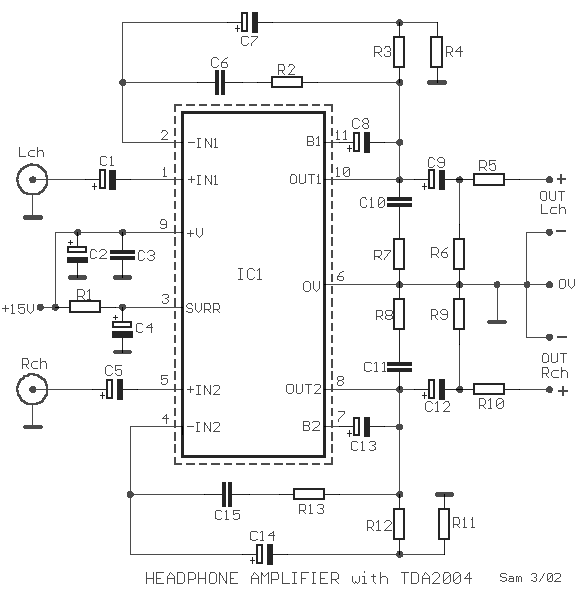
The operational amplifier circuit is designed to provide a reliable and efficient solution for driving headphones, particularly in applications where low load impedance is prevalent. The dual amplifier configuration allows for stereo output, enhancing the listening experience by delivering a balanced audio signal to each ear.
The voltage gain of 40 dB is achieved through careful selection of the feedback and input resistors (R3, R4, R11, and R12), which are crucial for maintaining the desired amplification level while minimizing distortion. The choice of resistors directly impacts the linearity and overall performance of the amplifier. The bandwidth limitation set at 22 kHz is sufficient for most audio applications, ensuring that the amplifier can handle the full range of audible frequencies without introducing significant phase shift or attenuation.
Impedance matching is critical in audio applications to ensure maximum power transfer and to avoid signal degradation. Resistors R5 and R10 serve this purpose by adjusting the output impedance of the amplifier to match that of the connected earphones, thereby optimizing performance.
The discharge resistors R6 and R9 play an essential role in the circuit's noise management. By discharging the coupling capacitors (C9 and C12) when the headphones are connected or disconnected, these resistors help eliminate pops or clicks that could otherwise disrupt the listening experience.
The power supply requirement of +15 V and a current draw of approximately 150 mA indicate that the circuit is designed for moderate power applications. The inclusion of a heatsink for IC1 is a necessary design consideration, as it helps dissipate heat generated during operation, ensuring the longevity and reliability of the amplifier.
Overall, this operational amplifier circuit is engineered to deliver high-fidelity audio output with low distortion and noise, making it suitable for a variety of headphone amplification applications. Proper layout and component selection are critical to achieving optimal performance and reliability in real-world scenarios.A opamp medium power, used as amplifier of headphones with possibility drive low loads. It contains in a nutshell two amplifiers. The voltage gain, has been determined in 40dB, from the R3-4 and R11-12, for each channel, respectively. The restriction of bandwidth for each unit is regulated by the combination of R12, C2 and R13, C15, in
22KHZ. The R5, R10 attend to the adaptation of impedance earphones. The resistors R6 and R9 discharge the capacitors C9 and C12, in order that when we connect the headphones in the plug, not we have annoying noise. The circuit has very good characteristics as low distortion, noise and satisfactory frequency response.
The requirement of circuit in current is 150mA, roughly, with voltage supply + 15V. The IC1 should be placed on a suitable heatsink. 🔗 External reference
Related Circuits
This is a simple, programmable, autonomous and extensible LED matrix with the possibility of being controlled by a computer using a RS232 connection. Its basic modules are the Controller Board, the I/O Port expander boards and the LED matrix...
The DC values of op-amp offsets cannot always be assumed to remain constant when delivering AC outputs. No device is perfectly symmetrical in terms of maximum positive slew rate compared to maximum negative slew rate. As a result, there...
A frequency signal tracking circuit is implemented using a phase-locked loop (PLL) configuration, which is a fundamental application of the CD4046 integrated circuit. The circuit, illustrated in the accompanying chart, utilizes the CD4046 to form a PLL that effectively...
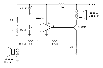
The example below illustrates the use of an operational amplifier (op-amp) as an audio amplifier in a basic intercom system. A small 8-ohm speaker is utilized as a microphone, which is connected to the op-amp input through a 0.1...

A simple audio watt meter circuit or an audio power or audio level meter circuit with diagram and schematics to measure amplifier audio output power in watts. The audio watt meter circuit is designed to measure the output power of...
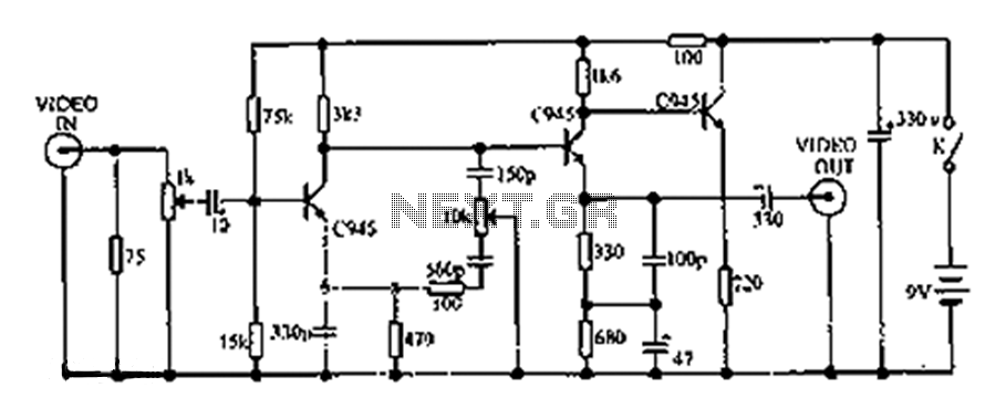
This circuit compensates for additional defects in image quality associated with LP (long play) recorders. The frequency components of the television signal reflect the details displayed on the screen. Enhancing the high-frequency components increases the edge sharpness of the...
Warning: include(partials/cookie-banner.php): Failed to open stream: Permission denied in /var/www/html/nextgr/view-circuit.php on line 713
Warning: include(): Failed opening 'partials/cookie-banner.php' for inclusion (include_path='.:/usr/share/php') in /var/www/html/nextgr/view-circuit.php on line 713