
High Input Voltage Linear Regulator
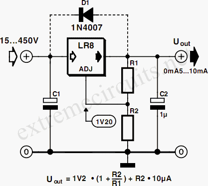
The LR8 voltage regulator is designed for high voltage applications, offering a significant advantage over traditional linear regulators. With its ability to handle input voltages up to 450V, it is suitable for a variety of applications, including industrial and automotive systems where high voltage levels are common. The adjustable output voltage feature allows for flexibility in design, accommodating different voltage requirements simply by changing the values of the external resistors R1 and R2.
The internal architecture of the LR8 ensures that it operates efficiently, with the nominal voltage difference of 1.20V between the Vout and ADJ pins being critical for the regulation process. The constant bias current of 10µA enhances the output voltage stability, making the LR8 suitable for precision applications.
In terms of protection mechanisms, the LR8 includes current limiting and thermal shutdown features, which are essential for preventing damage during overload conditions. The inclusion of diode D1 is crucial for safeguarding the regulator from reverse voltage scenarios, thereby enhancing the reliability of the circuit.
The recommended minimum output current and bypass capacitor specification ensure that the regulator performs optimally under varying load conditions. The calculation for the input capacitor C1 is particularly important for maintaining stability, especially in applications where the input voltage can fluctuate significantly.
The availability of the LR8 in different package types allows for versatile integration into various circuit designs, catering to both surface mount and through-hole assembly processes. The thermal performance of the packages further enhances their application in high power scenarios, ensuring that the devices can operate safely within their specified limits. Overall, the LR8 is a robust solution for high voltage regulation needs, combining flexibility, stability, and protection in a compact form factor.Commonly used 3-pin linear voltage regulators, for example the LM317, cannot handle input voltages in excess of about 30V. The LR8A from Supertex Inc is a new, adjustable three pin regulator that can accept input voltages up to 450V and can supply an output current of 0.
5mA to 10mA. Using this device it is possible to work with rectified 230VAC. T he LR8 has a wide input voltage range of +12 V to +450V. Two external resistors (R1 and R2) allow the output voltage to be adjusted from 1. 20 V to 440 V provided that the input voltage is at least 10 V greater than the output voltage. The LR8 adjusts the voltage difference between the Vout and ADJ pins to a nominal value of 1. 20V. This 1. 20V is amplified by the external resistor ratio of R1 and R2. An internal constant bias current of 10 µA is connected to the ADJ pin so that Vout is increased by a constant voltage of 10 µA times R2. The formula for calculating the output voltage is given next to the circuit diagram. To ensure stable operation of the regulator a minimum output current of 500 µA is necessary and a bypass capacitor of minimum 1.
0 µF should be used. Protection circuits in the LR8 limit the output current to 15mA typically and temperature protection ensures that the device temperature will not exceed 125oC. When the device reaches its temperature limit, the output voltage/current will decrease to keep the junction temperature within limits.
The two circuit diagrams show the LR8 used as a voltage regulator and as a constant current source. The current source can be used to a drive an LED. This con ¬guration would give an LED with super-wide input voltage range, i. e. , from +12V to +450V. The LR8 was originally designed to be used for switch mode supply start-up applications so it incorporates a feature which shuts down the LR8 when the output voltage exceeds the input voltage. Diode D1 is therefore necessary in the voltage regulator circuit diagram to prevent the output voltage exceeding the input voltage at any time.
The minimum value of the input capacitor C1 can be calculated from the following formula: C1(min) = (IL t ) / (Vpk Vout 10V) Where IL is the load current, and t the period between two voltage peaks. At 50 Hz, using one rectifying diode this will give a value t = 20 ms. Vpk is the peak input voltage, while Vout is the selected output voltage. The LR8 is available in two package outlines. The LR8N8 is a SOT89 SMD package while the LR8N3 is the familiar TO92 Transistor outline (e. g. BC 238). The TO-92 package can dissipate a maximum of 0. 74W while with suitable heatsinking, the SMD package can dissipate 1. 6W. 🔗 External reference
Related Circuits
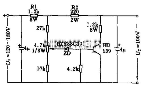
The circuit features no-load and short circuit protection mechanisms. To accommodate short circuit conditions, it is necessary to increase resistors R1 and R2 to allow for power dissipation; for example, R1 can be set to 1.2kΩ with a power...

A wideband high-frequency amplifier circuit is presented, utilizing resistance and capacitance coupling in a common emitter configuration to amplify high-frequency signals. When a high-frequency signal with an input impedance of 50 ohms is applied to the amplifier through a...
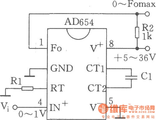
The circuit depicted is a low-cost voltage frequency converter (VFC) utilizing the AD654 component. By connecting the required components, Rl and Cl, as shown in the figure, a functional VFC application circuit can be established. The supply voltage can...
The DC to AC inverter circuit illustrated in the schematic is a straightforward design that produces a square wave output, which is sufficient to power various devices. The schematic diagram of the inverter circuit features a MOSFET configured as...
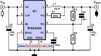
There are instances where a 5-V supply voltage is available, but certain components within the circuit require a lower voltage supply. In such cases, a voltage regulator from the Texas Instruments TPS62000 family is an excellent solution, particularly when...
Originally posted by Pano: "Like putting milk and sugar in your coffee. Next time by, your Turkish coffee comes with no sugar, Dave." The provided text appears to be an informal comment comparing the addition of sugar and milk to...
Warning: include(partials/cookie-banner.php): Failed to open stream: Permission denied in /var/www/html/nextgr/view-circuit.php on line 713
Warning: include(): Failed opening 'partials/cookie-banner.php' for inclusion (include_path='.:/usr/share/php') in /var/www/html/nextgr/view-circuit.php on line 713